Welcome to our site! EDAboard.com is an international Electronics Discussion Forum focused on EDA software, circuits, schematics, books, theory, papers, asic, pld, 8051, DSP, Network, RF, Analog Design, PCB, Service Manuals... and a whole lot more! To participate you need to register. Registration is free. Click here to register now.
U can use the HBM and MBM mentioned to build a test bench that measures the maximum current when the switch closes, and compare that current to the maximum current ur circuit can withstand.
simulation might give you some idea of the turn-on characteristic of the mos-clamps or diode strings, but due to the simulator and device modeling limitation, it won't predict accurate behavior after device breakdown, so you must collect data from silicon to know where your cliff is. and it is a tough job...
Here is basic HBM model,
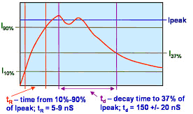
During HBM ESD testing, the HBM test circuit must apply a pulse that meets the requirements shown in Figure 2. The rise time of the HBM ESD pulse, tR, which is measured between the time the pulse reaches 10% of its peak current to the time the pulse reaches 90% of its peak current, must be between 5 to 9 nanoseconds long on the average. On the other hand, the time delay tD, which is the time it takes for the pulse to decay from 100% to 37% of its peak current, must be 150 +/- 20 nanoseconds long. The HBM pulse peak current at 400 V must be 0.27 +/- 10% A.
There is a canonical HBM ESD model. In simulation it's easy to
modify it such that the switch and capacitor are replaced with
a pulse source and series cap of same value. You could then
extend this to parameterized sources to enable full pin-pin ESD
performance analysis.
But it all depends on having a decent model of the clamp and
back-diode elements, which is not always available in the foundry
PDK.
Using a TLP and 'scope you can get short-time breakdown and
series resistance fitted. I use a degenerate zener model (forward
I-V and capacitance params are zeroed, so as not to affect the
presumably well modeled core clamp FET forward characteristics)
and fit the reverse characteristics so that the composite, clamp
+ "breakdown model", matches bench.
ESD clamps will walk in or walk out with repetitive stress. The
good ones will walk out (breakdown voltage increase, leakage
decrease) asymptotically; one that does the opposite is
unreliable and a poor choice. Maybe you only get one though.
Begin with the simple problem - does, or does not your clamp
element show a reasonable breakdown I-V, or is better than
reasonable (i.e. accurate)?
Now if you want to impress, find a way to simulate the Joule
energy shed in the clamp and its adiabatic temperature rise
(depending on device thermal mass <- volume <- params &
vertical details - SOI, etc.). And pay heed to current crowding
and the parasitic resistance mesh, which determine how well
you spread the power to keep the peak temp below damage
threshold. Of course you don't know this limit a priori, you
would determine it by a pulsed-power-to-blow series of zaps
on some test device, or devices employing different layout
styles to gauge best practices.
This site uses cookies to help personalise content, tailor your experience and to keep you logged in if you register.
By continuing to use this site, you are consenting to our use of cookies.