Continue to Site

Welcome to EDAboard.com

Welcome to our site! EDAboard.com is an international Electronics Discussion Forum focused on EDA software, circuits, schematics, books, theory, papers, asic, pld, 8051, DSP, Network, RF, Analog Design, PCB, Service Manuals... and a whole lot more! To participate you need to register. Registration is free. Click here to register now.

How does gain-boosting effect to output swing?

Status
Not open for further replies.

yonzzan

Junior Member level 3
Joined
Dec 12, 2006
Messages
26
Helped
0
Reputation
0
Reaction score
0
Trophy points
1,281
Activity points
1,522
0.18 micron technology vdsat

17_1172008666.jpg


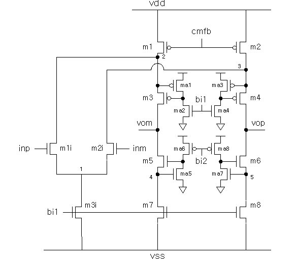
I am trying to decide effective voltages for each transistors in the figure.
In normal folded cascode, its output swing is derived by Vout=2( vdd-(vov1+vov3+vov5+vov7)).. which I am actualy unsure.

wil there be any change in the output swing calculation if I add gain-boosting part to folded cascode opamp?

Thanks ahead!!

Added after 1 minutes:

I have to meet this spec below.

Technology: TSMC 0.18 micron technology
DC gain:60dB
Gain bandwidth product:500MHz
phase margin 60
output swing 1vp-p
output load 2pF
slew rate 20V/usec
Fully differential op amp

Do you think that the topollogy above is the best choice?


Added after 2 minutes:

Also, how can I decide each Vb1, Vb2, Vcm..
Thanks
 

0.18micron folded cascode amplifier

In general, and unless you really know what you are doing, all transistors need to be in saturation. Given this in mind, the output swing will be calculated. To change from a folded cascode to gain boosting, the output of the gain boosting opamps should provide the required biasing to maintain the cascoded transistors in saturation. To summarize, I doubt that gain boosting will change the output swing for the same architecture. The reason I am saying this is that there are many ways you can do the gain boosting, but what people usually do, they don't use the same configuration you showed, rather, they use single stage for gain boosting to make the opamp faster. If you opt to go with the single stage approach, then yes, the ourput swing will suffer a little that the configuration you provided.

hope that helps...
 

60dB DC gain ? You should be able to get that without gain-boosting on that technology. Set input overdrive at 0.15V, and use 0.2 overdrive on every transistor from top to bottom, if your power supply is 1.8V then you'll have your
1V max output swing (so 2V peak differential amplitude, or 4V peak to peak, since your differential amplitudes goes from +2V to -2V).

You can always push more current thru the input device to get the gm you'll need for the 500MHz GBW and the given load capacitance.

The gain-boosting that you show will reduce the max ouput swing, btw. Use another kind of auxiliary amplifier if you want to do that.
 

I think you might have some hard time trying to get the gain with a relatively high GBW. Anyway, I strongly suggest you give it a shot. If the first iteration brings you close enough, then it is better to spend time tweaking the biasing and sizes than designing a gain booster.

To answer your question: your gain boosters are fully differential amps, which means that a CMFB is needed for each gain booster. I suggest a single ended amp for each cascode transistor.
 

In general the active regulated cascode is the right choice for solving the trade between DC gain and output voltage swing. BUT

THIS ARCHITECTURE IS BAD! WHY?

Because the voltage across source/drain of m1 is vth-vdsat(ma1). That is higher than vdsat(m1). So you need a different amplifier.

You can use instead of ma1 a NMOS source follower with the same ma1. That shift the drain voltage of m1 near the optimum point. I prcatical found the best voltage for m1 is 1.5*vdsat(m1). You have to design the bias network to get to this point which is difficult because the vdsat of ma1 depend then on vth of a NMOS.

The next better circuit is to use a NMOS diffamp instead of the NMOS source follower. The PMOS mirror output of the NMOS diffamp is connected to a NMOS source follower to shift the voltage. The souce follower output is connected to the m2 gate.

The third solution uses a NMOS diffamp with a folded cascode output. That is what is built in most boosted cascodes.

The high frequency operation is not much affected by the boost amp structure. But the dimension of m1 & m2 could now be made near minimum lenght and that reduce the parasitics of m1 and m2. So for the same voltage swing and DC gain the parasitc pole is higher. So you can shift the trade point to higher level.
 

Status
Not open for further replies.

Part and Inventory Search

Welcome to EDABoard.com

Sponsor

Back
Top