Vabzter
Member level 1
Hi all,
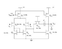
Please refer the following diagram of two stage opamp..Vdd = 1.8V, Vbias = 1.234V, Cload = 35pF
When I give 900mV as input to both input terminals the output is 900mV and all the transistors are in saturation.
My problem is:
1When I connect it in non inv. config. with resistive feedback(Rf = 1K, R1 = 1K) I get 100mV out if input is 1V..Not working as amplifier..
2. How to find the offset voltage of opamp in cadence
Thanks in advance
BR
Vabzter
Please refer the following diagram of two stage opamp..Vdd = 1.8V, Vbias = 1.234V, Cload = 35pF
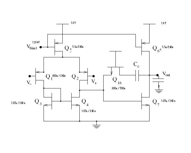
When I give 900mV as input to both input terminals the output is 900mV and all the transistors are in saturation.
My problem is:
1When I connect it in non inv. config. with resistive feedback(Rf = 1K, R1 = 1K) I get 100mV out if input is 1V..Not working as amplifier..
2. How to find the offset voltage of opamp in cadence
Thanks in advance
BR
Vabzter