Continue to Site

Welcome to EDAboard.com

Welcome to our site! EDAboard.com is an international Electronics Discussion Forum focused on EDA software, circuits, schematics, books, theory, papers, asic, pld, 8051, DSP, Network, RF, Analog Design, PCB, Service Manuals... and a whole lot more! To participate you need to register. Registration is free. Click here to register now.

How about this bandgap current source?

Status
Not open for further replies.

Davidy

Junior Member level 2
Joined
Sep 14, 2005
Messages
21
Helped
0
Reputation
0
Reaction score
0
Trophy points
1,281
Activity points
1,465
Who can help me the analysis this bandgap circuit?
56_1162124863.GIF

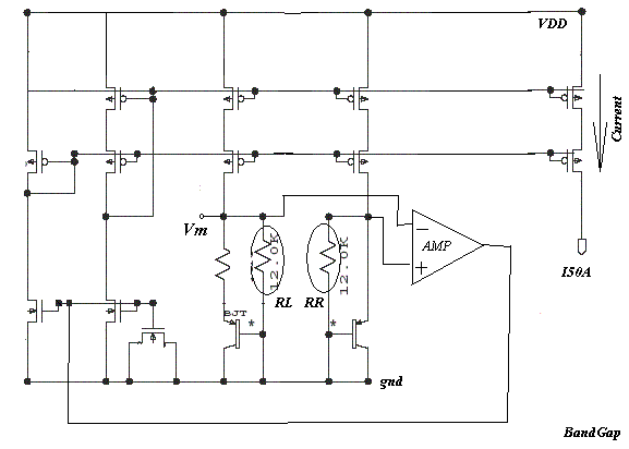
1.How about the current "I50A" in this bandgap circuit?
Is it PTAT current or temperature-independent?
I think it is PTAT but I was told that it work as a bandgap current source in a ADC circuit.

2.How about the voltage "Vm" in the middle of the circiut?
Is it PTAT current or temperature-independent?

3. What is the usage of the two resistors "RR" and "RL" in the base terminl of the bipolor FET?

Thx!
 

1. It should be a temperature-independent current source if you compensate not only VBE, Delta VBE but also the temp coef. of resistors.
The current I50A is equal to the sum of VBE/RL and (Delta VBE)/RX, whereas the RX is the resistance of the resistor between node Vm and BJT.

2. Vm = VBE of the BJT.
3. To get the voltage VBE and produce a current VBE/RL or VBE/RR.

The following is a similiar schematic.
63_1162178283.gif


Your schematic seems be a somewhat twisted version.
Here comes my problem: Is there any advantage to use your schematic instead of mine?
 

    Davidy

    Points: 2
    Helpful Answer Positive Rating
I think you can refer to this paper "H. Banba, H. Shiga, A. Umezawa, T. Miyabata, T. Tanzawa, S. Atsumi, and K. Sakuii, “A CMOS bandgap reference circuit with sub-1-V operation,” IEEE J. Solid-State Circuits, vol. 34, pp. 670–674, May 1999."
 

ycj said:
1. It should be a temperature-independent current source if you compensate not only VBE, Delta VBE but also the temp coef. of resistors.
The current I50A is equal to the sum of VBE/RL and (Delta VBE)/RX, whereas the RX is the resistance of the resistor between node Vm and BJT.

2. Vm = VBE of the BJT.
3. To get the voltage VBE and produce a current VBE/RL or VBE/RR.

The following is a similiar schematic.
63_1162178283.gif


Your schematic seems be a somewhat twisted version.
Here comes my problem: Is there any advantage to use your schematic instead of mine?

Thank you.
I think my circuit will have bigger PSRR becasue of the cascode current mirror and another voltage subtractor.
Can you tell me which paper does your circuit from?
I am a little curious about the third terminal of the opa in your circuit.

Added after 1 minutes:

qiushidaren said:
I think you can refer to this paper "H. Banba, H. Shiga, A. Umezawa, T. Miyabata, T. Tanzawa, S. Atsumi, and K. Sakuii, “A CMOS bandgap reference circuit with sub-1-V operation,” IEEE J. Solid-State Circuits, vol. 34, pp. 670–674, May 1999."
Thank you!
I will read your recommented paper.
 
Last edited by a moderator:

The original purpose of the circuit is voltage reference.
To use it as temperature compensated current reference, the temp. coef. of the R should be considered.

See the following link:
 

I think maybe there is something wrong with your schematic, maybe it is just a typo, because all the PFETs' gates on the top of your schematic have been connected to Vdd.
 

Davidy said:
I think my circuit will have bigger PSRR becasue of the cascode current mirror and another voltage subtractor.
Hi,

I can't figure out the subtractor in your schematic. Can you please point me out?

Or is it added externally?

Regards
 

The AMP requir it's positive input and negative input's voltage level should be
equal , so :
Vbe1 + I*R = Vbe2 ,
and then , we get :
I= Vt/R * lnA , A= emitter area ration of PNP1 to PNP2 .

The negative control process :
When the negative input of the AMP is low than the positive , the AMP's
output increase , so the currents in the PNPS will increase too . For Vm,
it equal to the sum of voltage cross the resistor and the Vbe1 . By making
this voltage larger than the Vbe2 , we get the result that the negative input
of the AMP increas more than the positive input .
 

ycj said:
The original purpose of the circuit is voltage reference.
To use it as temperature compensated current reference, the temp. coef. of the R should be considered.

See the following link:

Thank you!
I got it.

Added after 3 minutes:

ipsc said:
Davidy said:
I think my circuit will have bigger PSRR becasue of the cascode current mirror and another voltage subtractor.
Hi,

I can't figure out the subtractor in your schematic. Can you please point me out?

Or is it added externally?

Regards

The 'subtractor' is refered to the left common source circuit which is the output of amp.
This name is from a paper of TI's engineer.
 

Davidy said:
ipsc said:
Davidy said:
I think my circuit will have bigger PSRR becasue of the cascode current mirror and another voltage subtractor.
I can't figure out the subtractor in your schematic. Can you please point me out?

Or is it added externally?
The 'subtractor' is refered to the left common source circuit which is the output of amp.
This name is from a paper of TI's engineer.

The left part is commonly used wide-swing bias mechanism. It performs the job of subtractor to an extent, though it's not a complete/perfect subtractor. I thought you might be using some subtractor, which is not given in figure.

Regards
 

Status
Not open for further replies.

Part and Inventory Search

Welcome to EDABoard.com

Sponsor

Back
Top