Youncen
Member level 2
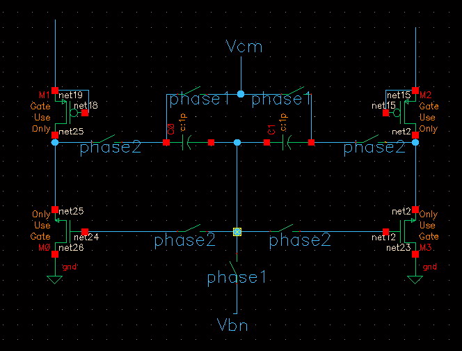
as in the picture,when phase 1 come, Vcm and Vbn create a voltage difference on the capacitor,when phase 2 come,the voltage difference is feedbacked to the lower transistor pair,and phase1 and phase 2 do not overlap
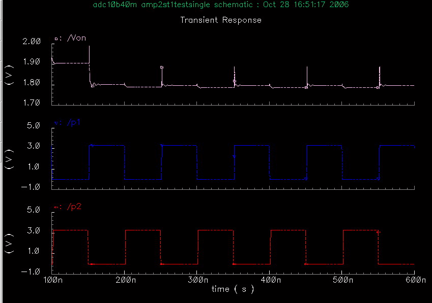
but the simulation gives this result, periodic output dc level and some ripples,my god!
(the result pic,p2 is actually phase1 ,and p1 is actually phase2 ,sorry for my mistake)
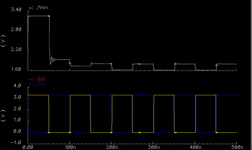
after I tuned the complementary mos switcher's w and l,(I guess the main reason is that the pmos' charge injection is greater than the nmos'),the result turned to be this ,the uneven voltage level is alleviated ,but still some over drive pulse exist,is it caused by the clock feedthrough ? can any one offer some sugestion?,or tell me how this unstable common output will affect my opamp