Continue to Site

Welcome to EDAboard.com

Welcome to our site! EDAboard.com is an international Electronics Discussion Forum focused on EDA software, circuits, schematics, books, theory, papers, asic, pld, 8051, DSP, Network, RF, Analog Design, PCB, Service Manuals... and a whole lot more! To participate you need to register. Registration is free. Click here to register now.

vco with replica biasing for pll

Status
Not open for further replies.

ranilf

Newbie level 3
Joined
Mar 24, 2006
Messages
4
Helped
0
Reputation
0
Reaction score
0
Trophy points
1,281
Activity points
1,338
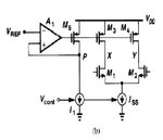
Hi I am designing a vco with replica biasing and have a few questions. For the design, I'm using a differential design as in the picture below. This was taken from Razavi's book. Now to the problems. I can't seem to get the replica bias to work properly, as the Vds value from the pmos in the replica bias never matches the load pmos in the diffamp. I have tried setting all the pmos in saturation and also all in linear but nothing seems to work. So here are a few questions:

1) Should the pmos be in linear region or can they be in saturation when acting as a resistor. Or do they have to be in deep triode region as the Razavi book says.
2) Also, any tips for biasing the transistors. I am using VDD = 3.3v and .35 micron technology
3) What is a good value for Vref to be.
4) Finally, should Iss and I1 be the same value, or should I1 be half the current of Iss since this is a half replica?

Thanks guys, and I would really appreciate any help as I've been stuck on this for a long time.
 

Attachments

  • vco_1219.jpg
    vco_1219.jpg
    20.7 KB · Views: 437

hi actually i used the maneatis delay cell instead and got it working at 500mhz with everything in saturation. what is the best way to convert the vco output into a square wave which will go back to the pfd. will a simple comparator, like a opamp, work?
 

pmos transistor should be act as a resistor,so it should in the triode region for full tuning range.
and iss and i1 shud be the same current mirrors,so that they will tack the current variations.,
use a high gain opamp as the erroramp,so that it will always makes u r erorvoltage low.
vref= vdd-vsw.
u find out u r swing value from u r application,what is the min,and max voltages your output shud be.
 

everything in saturation?

no, it is not right. Maneatis load should not be all in satiration region.
U may not understand maneatis load's theory.

u need a buffer first to increas the vco swing
and then followed a comparator.
buffer can have the same structure as ur vco cell.


ranilf said:
hi actually i used the maneatis delay cell instead and got it working at 500mhz with everything in saturation. what is the best way to convert the vco output into a square wave which will go back to the pfd. will a simple comparator, like a opamp, work?
 

hi thanks for the input. so i guess i need to have the pmos load in linear region always and the diode connected pmos should obviously be in saturation. but does that pmos load always have to be linear, because i asked my teacher and she said it can be in saturation as well as it gives a bigger resistance value. but anyways i am going to have my vref at 2.3 v, so a voltage swing of 1 v. how much current is normally necessary and what should generally be the pmos/nmos size ratio?
 

Vds will never match in this case since in replica leg, you just have one PMOS transistor. If you really want vds to match, add replica NMOS in replica circuit. The pupose of the replica circuit is two fold:

1. To track any variations. If there are any current/power supply variations, replica circuit and error correction opamp will pull biasing point to stable values set by Vref
2. To set output swing. Lowest value on X,Y will be Vref. Hence max swing you can have at output of this circuit is vdd to vdd-vref.

For faster speed, you will like to use smaller swing and keep devices into linear region. To keep PMOS in linear region, you need to set vref at least equal to vdsat of M1,M2 and current source. ISS,I1 can be same or you can scale current I1 and PMOS M5 by same factor.

Hope this helps.
 

thanks for the tips.i actually got it to work with an output swing of 2.7 to 3.3 v. and my vref is 2.7 so that seems right. one last question though. i made a two stage opamp (diff to single ended) that takes a sin from 2.7 to 3.3 and shifts it down to a common mode of 1.65. so it is supposed to swing from 1.35 to 1.95. i did this so then i can put that through an inverter and get rail to rail swing from 0 to 3.3, which will go to the pfd. i tested this opamp by itself and it does the job of shifting down to cm of 1.65, but when i connect this opamp to the output of the vco, the vco stops oscillating. anyone know why?
 

Hi All,

can you please help me in designing Maneatis delay cell for DLL.
i have few queries :

1.How the Symmetric load works.
2.With linear load how the dynamic supply variation improves.
3.How the delay varies with control voltage.
4.In Maneatis delay ,the swing is also varying with VCTRL ?
5.What it means by dynamically we are adjusting the BIAS current with VCTRL to reduce the Power supply noise.
6.do u have any good material related to power supply noise, and how with the linear load we can achieve a better noise tolerance.


thanks.
 

Status
Not open for further replies.

Similar threads

Part and Inventory Search

Welcome to EDABoard.com

Sponsor

Back
Top