akbarza
Full Member level 2
hi
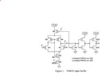
in attached pic(from article:K. Duwada, V. Saxena, R.J. Baker, High speed digital input buffer circuits, in 2006 IEEE Workshop
on Microelectronics and Electron Devices, 2006. WMED’06 (IEEE, 2006), pp. 2-pp)
1) is the buffer used as an analog buffer or digital buffer? in title of article is written for digital. why isn't used two cascade inverters as digital buffer?
2) in the article is written the following sentence:
"The input buffers are designed with ‘enable’ logic using the
NMOS and PMOS switches, like M5B and M6 in fig.1 controlled by signals Vs and Vs_bar . When the enable signals are
off, the output of the diff-amp will be in high impedance state.
This can cause a large amount of current to flow in the
inverters and damage the chip. To avoid this scenario, a switch
M7 is connected to the output of the diff-amp which clips the
node to ground when the buffer is disabled. ,"
please explain more about it. why the output resistance of diff_amp will be high when M6, M5B are turned off? from where the mentioned current com?( there is not any way to supply voltage)
3) can i use an op-amp in unity gain structure as an analog buffer?
thanks
