Continue to Site

Welcome to EDAboard.com

Welcome to our site! EDAboard.com is an international Electronics Discussion Forum focused on EDA software, circuits, schematics, books, theory, papers, asic, pld, 8051, DSP, Network, RF, Analog Design, PCB, Service Manuals... and a whole lot more! To participate you need to register. Registration is free. Click here to register now.

VCO phase noise problems

Status
Not open for further replies.

hanikapa

Member level 4
Joined
Feb 6, 2015
Messages
71
Helped
0
Reputation
0
Reaction score
0
Trophy points
6
Activity points
510
Hi,
I have the measurement results for an LC-VCO which is working at 2GHz and the design is based on conventional structures. The measured phase noise is -90dBc/Hz but the simulated phase noise using RC extracted design is -110dBc/Hz. Does anybody have experience that why the phase noise is much worse?

- - - Updated - - -
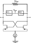
vco.png
The above picture is the structure for the designed VCO
 

There may be many reasons such as..
-Lower Quality Factor of the Resonant circuit than preview
-Poor Noise model of the active devices ( MOS,Varactor)
-Underestimated Supply Noise ( VCC and Vtune)
-Measurement and Calibration Errors
-Poor GND decouplings

etc.
There may few more..It's not easy to predict the main cause without deep information about the circuit and measurement set-up.
 
This oscillator may have more than one mode of operation. Current flow may go around a large loop, or two loops. There might be a middle state of action in between. Action may or may not be symmetrical. Therefore measurements can be different depending on what mode you catch it operating in.
 
Do you know how can this problem be solved? The VCO is used in a PLL loop.
 

The phase noise is measured at 1MHz offset frequency.

@1MHz is generally related to VCO PN itself. ( But I don't know the Bandwidth of the PLL Loop Filter ) So if we assume that is Out-of-Band PN, it will absolutely come from VCO so you should concentrate on VCO PN.There may be many reasons as I have mentioned before but you should examine it in the light of my suggestions.
 
Are your simulations settings accurate? How did you extract inductor? Are you using any electromagnetic simulator(Sonnet, EMX etc.) for your inductor model? 20 dB is a huge difference.
 

Have you measured phase noise with Vtune pinned
to a dead-quiet midrange voltage?

Have you observed the character of the noise slope
at points other than 1MHz offset? To see if it's 1/f,
contains spurs, has any other signature that might
implicate a particular source(s)?

Have you measured supply noise spectrum and
determined whether this, convolved with PSRR(f),
explains the excess?
 
I use cadence calibre RX to extract the oscillator.
I measured the phase noise of the PLL and concluded from it the phase noise of the oscillator. So, I did not measure the oscillator alone to see the effects that dick-freebird mentioned.
 
Last edited:

Calibre for VCO core circuitry. For Inductor, I assume you have used a 3D simulator as I mentioned in my previous post. You need to check the effect of BW on phase noise to conclude its source.
 

The vco output is going to a 50 ohm buffer and the output of buffer is measured for the phase noise. In simulations, I had to use external passive elements to get to 50 ohm matching but for the measurements, the probe is direcctly connecting to the output without these elements. do you think that this can have effect on phase noise measurements?
 

A 'scope probe with its ground loop will pick up all kinds
of ambient EM noise. You could look at the output of a
grounded-input buffer via 50-ohm cable and see what
the noise amplitude and spur frequencies look like, and
then connect the VCO to the buffer while leaving the
rest of the lineup as-was, perhaps this will eliminate
some pickup (and the rest, would be known so you can
try a "reverse superposition").

What 'scope probe passes 2GHz without gross attenuation?
That's another question.
 
I think hanikapa uses IC wafer probes, not PCB scope probes.

Can we see a plot of measured phase noise?
 
After doing more investigations, we understood that the jitter of the design has a large dependency on the external decoupling capacitor of the VCO. Does anybody have any idea??
 

This is true, and getting decoupling close-in enough
to help at high frequencies (L kills C, and pulls in SRF
of the decoupling "tank") would be a primary challenge.
At a minimum look at adding shunt C to the probe card
(if we're talking wafer probe) or even chip-on-chip
(an epoxied-down chip cap, skip-bonded to the pads,
hopefully leaving enough room for probe tips).

Maybe you could be more clear about the sample and
hardware physical details.
 
just another question is about simulating the phase noise. I use PSS and Pnoise in cadence. Are the results taken from them reliable to compare with measurements?
 

They may be reasonable as far as self-generated
phase noise. But everything is only as good as the
models, including externalities (whether, or how well
noise sources, loops, impedances and such are
represented).

You might drill into the foundry PDK docs for some
sort of model-vs-silicon report and see if noise model
accuracy gets any mention, and whether this extends
to newer RF noise analyses or just classic SPICE noise
small signal analysis. The tools work when people make
them work. To be proven, not assumed, when it comes
down to cases.
 
Status
Not open for further replies.

Part and Inventory Search

Welcome to EDABoard.com

Sponsor

Back
Top