Continue to Site

Welcome to EDAboard.com

Welcome to our site! EDAboard.com is an international Electronics Discussion Forum focused on EDA software, circuits, schematics, books, theory, papers, asic, pld, 8051, DSP, Network, RF, Analog Design, PCB, Service Manuals... and a whole lot more! To participate you need to register. Registration is free. Click here to register now.

[USB] Reverse current protection.

Status
Not open for further replies.

franekz

Junior Member level 2
Joined
Dec 10, 2015
Messages
20
Helped
2
Reputation
4
Reaction score
2
Trophy points
3
Activity points
155
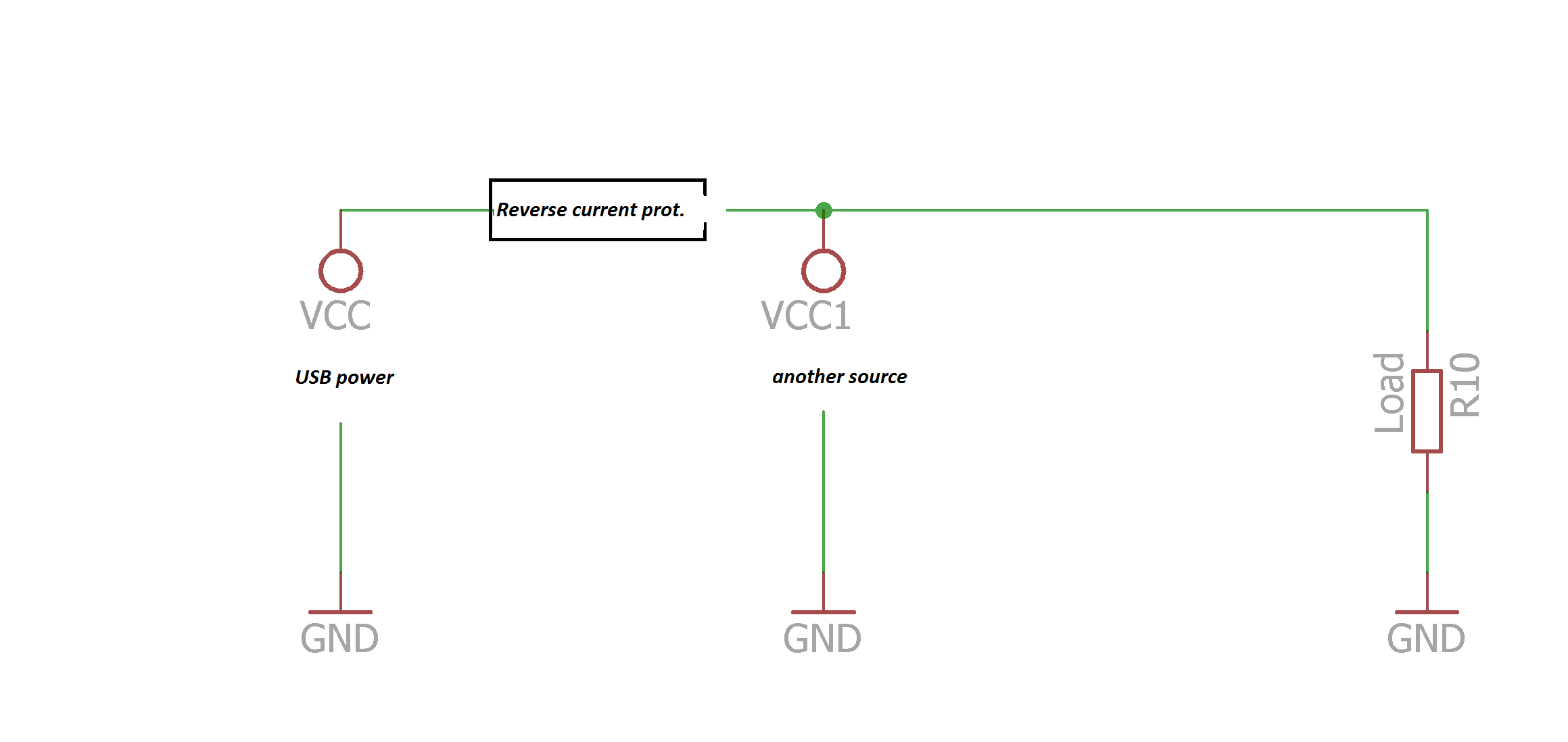
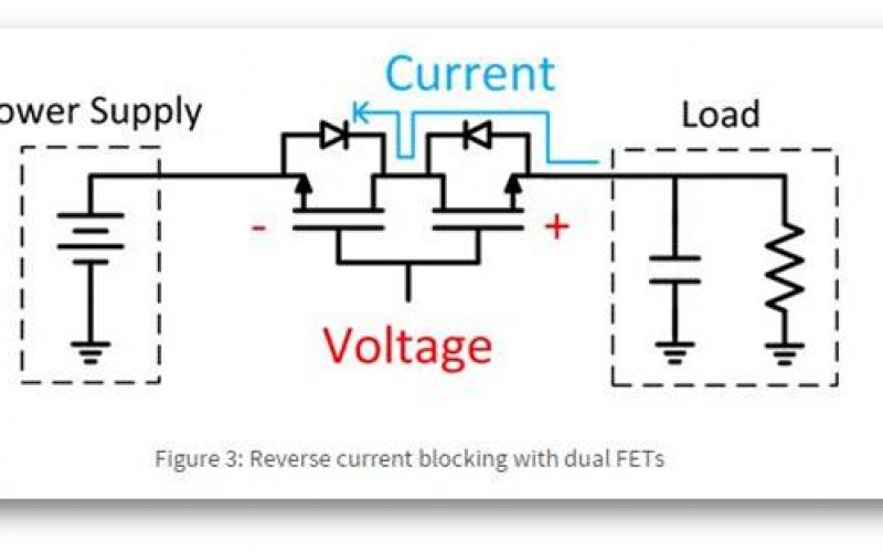
Hi Guys, I work now on a dual power design: USB and mains. I need to protect USB power line against a reverse current flow, but the simplest methods (diode, Schottky) have quite high voltage drop. Is it a good idea to use P-channel MOSFET? Will be the voltage drop lower? Or maybe some other ideas?

Unfortunately it is a quite "price sensitive" design and I look for not to expensive solutions.

Thank you
Peter
 

Hi,

A simple P Mosfet won't do. It needs some extra logic.

I'd look for "ideal diode" IC. There are some especially made for USB application.

If you want to build a discrete solution, then post your idea as schematic. Then we can discuss on it.

Klaus


Vcc is the usb power.
Vcc1 is an another supply.

Protection device should stop current from flowing towards the Vcc from Vcc1 if Vcc1 > Vcc.
 

Attachments

  • double.png
    double.png
    28.9 KB · Views: 87


This double NMOS FET solution seems elegant, but needs a switched gate Voltage supply depending on which side the voltage is more positive: for the normal supply-to-load direction a voltage several volts higher than the supply voltage to well open (both) channels, for the reverse direction protection the gate has to be switched to GND in order to cut off both channels.

Actually a similar argument is valid for the very simply-seeming high-side backward-connected PMOS FET protection of Figure 5 in your above presented Maxim-link: for the normal supply-to-load direction the given description is correct (the low-ohmic channel way may lower the voltage drop below the p-n junction drop), but in case of reverse voltage the fixed gate-to-GND connection doesn't help against reverse current: indeed the parasitic bulk-to-drain junction diode is cut-off, but the channel is still open! (Check the gate-to-source voltage!). For real reverse current protection, the gate connection has to be switched to the source.

In promotion of a really simple solution, I'd vote for a Super Barrier Rectifier (check G00GLE). Use a 10-to-20-fold current capability than you actually need, and your voltage drop will be down to 300..400mV only, see e.g. these SBRs @ DigiKey: you can get a 10A SBR (both diodes in parallel) for about 34¢ in volumes of 50.
 
This double NMOS FET solution seems elegant, but needs a switched gate Voltage supply depending on which side the voltage is more positive:
Yes I know. I consider use of a comparator to do this task.
 

Yes I know. I consider use of a comparator to do this task.

With the NMOS FET solution you always need an additional few volts more positive gate voltage than your power supply voltage to drive the NMOS FET(s) into triode region (and so achieve a smaller voltage drop than the parallel p-n junction provides). If you just need reverse-current protection, the 2nd (right) NMOS FET is redundant and just adds more voltage drop. You only need the backward-connected (the left) one.

With a (for the same voltage drop more expensive) also backward-connected (drain at the power supply side) PMOS FET you wouldn't need the higher gate voltage - you just switch its gate connection between GND (PMOS FET open) and source (VCC1), FET cut-off then.

Thinking of simplicity, cost, and comparing voltage drop, I don't think you could get the FET solution for less cost than for such an aforementioned SBR or even a (power) Schottky diode. And you'd spare the comparator and its routing.
 

Here's a reverse protection circuit using an N-MOSFET and a comparator to act as an ideal diode and block reverse current through Vcc.
It's ON voltage drop is just the output current times the MOSFET ON resistance

I put the MOSFET in the negative leg so a cheaper N-MOSFET and a common LM 339/393 comparator that can work on ground based voltages can be used. (That comparator input can't work at the high side voltage.)

The comparator monitors the voltage at the MOSFET drain and when the drain voltage is negative, indicating normal current direction through Vcc, the comparator output is positive, turning on the MOSFET.
If the voltage goes positive, indicating the current is reversing through Vcc, the comparator output goes low, shutting off the MOSFET to prevent reverse current through Vcc.

Note that the normal current flow for this circuit is through the N-MOSFET from source to drain.
This works because MOSFETs conduct equally well in either direction when ON.

D1 is for simulation purposes, to prevent reverse current through Vcc1 when the Vcc1 voltage is lower than Vcc's.
Note that, for 5V operation, the MOSFET must be a logic level type where the Rds(on) is rated for a Vgs of 5V or less.

The LTspice simulation shows the comparator output voltage and the VCC current going to zero when Vcc1 (plus the diode drop) exceeds Vcc.

Capture.PNG
 
Last edited:
Hi, Thank you
The only one problem with this circuit. The MOSFET is on the low side, and the GND will flow. I need it stable as I use ADCs in my project. I was looking for something which is on the high side of the circuit.
 

....
The only one problem with this circuit. The MOSFET is on the low side, and the GND will flow. I need it stable as I use ADCs in my project. I was looking for something which is on the high side of the circuit.
The only problem is your perception of that as being a problem.
Whether the MOSFET is in the high side or the low side, it will have the same effect on the supply voltage between power and the ground reference point.
Note that the ground point is on the right side of the MOSFET so it will not affect any of the voltages referenced to that ground point.

Remember ground is just a reference point, there's nothing else special about it.

If you put all the circuitry to the left of D1 inside a black box with just the two outputs, there would be no measurement you could do that would tell you whether the MOSFET was in the plus side or the minus side inside the box.
 
Last edited:

Status
Not open for further replies.

Similar threads

Part and Inventory Search

Welcome to EDABoard.com

Sponsor

Back
Top