ashrafsazid
Advanced Member level 4
Hi,
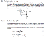
Can anybody help me out suggesting how I can implement the circuit shown below on transistor level? The main thing I want to know how can I implement this Voltage Controlled Voltage Source (VCVS) of gain 1 and gain 30 respectively.

Can anybody help me out suggesting how I can implement the circuit shown below on transistor level? The main thing I want to know how can I implement this Voltage Controlled Voltage Source (VCVS) of gain 1 and gain 30 respectively.