Continue to Site

Welcome to EDAboard.com

Welcome to our site! EDAboard.com is an international Electronics Discussion Forum focused on EDA software, circuits, schematics, books, theory, papers, asic, pld, 8051, DSP, Network, RF, Analog Design, PCB, Service Manuals... and a whole lot more! To participate you need to register. Registration is free. Click here to register now.

Logic function of circuit with diodes and transistors

Status
Not open for further replies.

userXY

Junior Member level 1
Joined
Feb 9, 2017
Messages
19
Helped
0
Reputation
0
Reaction score
0
Trophy points
1
Activity points
193
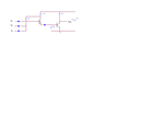
For the circuit in attachment1, determine the logic function and minimum resistance value of the resistor Rcmin such that the output transistor is in saturation state when it is on.
If the output transistor is charged with capacitor Cp=220nF, determine the fall and rise time of the output voltage.
Given data: βmin=50, β=100, Vcc=5V, Ubet=0.5V, Ubes=0.7V, Ube=Ud=0.6V, Uces=0.2V.

Note: This is not homework, I am practicing for exam.

Attempt:
We consider the static analysis of a circuit (low and high logic level).

Note: I assumed that diodes are idealized (when it is forward biased the voltage is 0.6V, and when it is reverse biased, it is an open branch).

1. Low logic level (Vin=0V)
We don't consider this case because we can never have Vin=0V.
Is this correct?

2. High logic level (Vin=Vcc=5V)
We conclude that at least one input diode is forward biased.
Fourth diode (that is connected to emitter of input voltage) is reverse biased.
Output transistor is on. We need to check if it is in saturation state.
The condition is Ics>Ib/βmin. We can find Ib as Ib=Ubes/5k=0.14mA and Ics as Ics=Uces/Rcmin. This gives that Rcmin>200/7 Ω.
Is this correct?

Where to connect capacitor Cp and how to find fall and rise time of Vout?
What is the value of Vout in this case?
 

Attachments

  • attachment1.png
    attachment1.png
    10.6 KB · Views: 88

Hello.

1. Low logic level (Vin=0V)
We don't consider this case because we can never have Vin=0V.
Is this correct?

No, you can actually have any voltage there. In the circuit it's connected to air, which would be a very low voltage white noise or something. We will assume that these inputs will only work with 0 or 5V.
So yes, it can be 0V, if you connect them to ground they will actually be in 0V.

Fourth diode (that is connected to emitter of input voltage) is reverse biased.
It's actually not even biased. Not forward, not reverse, because both potentials are theorically zero. Maybe in real life there's a few houndred of milivolts, but the diode won't polarize neither. Then the output transistor base is at 0V and the transistor is OFF. Because of that, the output is "high".


Where to connect capacitor Cp and how to find fall and rise time of Vout?
What is the value of Vout in this case?
I would assume that the capacitor is connected between Vout and GND. That will make the output to rise and fall slower than without the capacitor.
This rise and fall times are how much it takes the output to reach 90% of the opposite state.

RISE transient:
The cap will charge through a 6K resistor.

Vc= Vi + Vf * e^(-t/(R*C)). --> Charging Formula

Vc = Vi + Vcc * e^[t/(6K*220uF)].

Vi is the initial voltage of the capacitor. It will be Uces=0.2V. Vcc is 5V. "t" is what you have to calculate. Replace "Vc" by 90% of 5V (4,5V) and find "t". Apply "ln" (e base logarythm) to both terms to "eliminate" the "t" from the exponent. Do your math.


FALL transient:
The cap will discharge only through the transistor which ideally won't have any resistance (it does), but as it's not specified you should assume that the fall time is zero.


The logic function is NAND.
 

How did you conclude that the logic function is NAND?
 

Hi,

How did you conclude that the logic function is NAND?

All inputs must be HIGH --> then the output becomes LOW
In any other case the output is HIGH.

This is called NAND function.

Klaus
 

What about the value of Rcmin ? Is it correct?
 

Looks like a three input NAND gate to me.

If the inputs are high, the input diodes are reverse biased and do not conduct. That leaves the first transistor conducting and passing current to the base of the second one so it's collector is LOW.

If one or more inputs goes LOW, the first transistor loses its bias, stops conducting so the second transistor turns off and it's collector goes HIGH.
So the truth table is:
a b c out
0 0 0 1
0 0 1 1
0 1 0 1
0 1 1 1
1 0 0 1
1 1 0 1
1 1 1 0

The middle diode is there to ensure that when an input goes low, the first transistor is completely shut off because it's base has a lower potential than it's emitter. Without it, there would be a risk of leakage leaving some conduction.

The other parameters depend on the transistors but basically, the rise and fall times are just the RC time constants of the load resistors and junction/wiring capacitance. An active drive circuit to the output transistor would improve speed by sinking base charges instead of relying on the 5K resistor to do it.

Brian.
 

In about 1967 I worked with an office computer that used these DTL circuits in ICs. Then came TTL then came Cmos logic ICs.
 

In about 1967 I worked with an office computer that used these DTL circuits in ICs. Then came TTL then came Cmos logic ICs.

In 1967, we had in our physics class the experiment on diodes- curve tracing. It was a vacuum tube and we have heard about the solid state diode in the theory class. Our teacher struggled to explain why the diode conducts in one way only.
 

Status
Not open for further replies.

Part and Inventory Search

Welcome to EDABoard.com

Sponsor

Back
Top