Continue to Site

Welcome to EDAboard.com

Welcome to our site! EDAboard.com is an international Electronics Discussion Forum focused on EDA software, circuits, schematics, books, theory, papers, asic, pld, 8051, DSP, Network, RF, Analog Design, PCB, Service Manuals... and a whole lot more! To participate you need to register. Registration is free. Click here to register now.

Manage with different voltages from super cap

Status
Not open for further replies.

benji54

Newbie level 5
Joined
Aug 6, 2016
Messages
9
Helped
0
Reputation
0
Reaction score
0
Trophy points
1
Activity points
80
Hi everyone,
I am wondering how I can manage with different voltages from different super cap.
I explain the schematic below, I have 4 supercap (400mF rated 3.3v) that are charged by different controlers from generators. This means that at a time T1s the C1 could provide maybe 3.24V if it is fully charged or 1.24v if not, same for C2 and C3 (0 to 3.3v) and C4 between 3.2-1V. My problem is that I want to supply a low power microcontroler using the energy available on fourth capacitors.
If I connect all the capa together it means that the voltage will equalize itself, that why I put a diode after each supercap to get no current reverse from a super cap to another one. Is this schematic can work?
New-Project.png
 

Hi,

There are circuits called "ideal diode". Maybe this is a good way.

Or measure all voltages and select the highest one with a cmos switch.

Klaus
 

Thank you,
And what about an another supercap which will be charged by these different supercap?It will be the same
 

Hi,

There are circuits called "ideal diode". Maybe this is a good way.

Or measure all voltages and select the highest one with a cmos switch.

Klaus

The things is I want to power supply a low power microcontroler with the energy available so put another circuit which consums current to select the highest voltage seems too much...
 

Hi,

ideal diodes circuits, cmos switches and Mosfets draw very low power.

A simple solution could be to use a P-CH Mosfet for each capacitor.
A high impedance resistor acgoss GS
Drain to capacitor, Source to load. Gate low = ON, gate HIGH or highZ = OFF (body diode)

Look for low V_GS_th mosfet.

Klaus
 

An ideal diode requires an active circuit that monitors the MOSFET voltage drop. Schottky rectifiers might be a suitable solution, too.


Hi,

ideal diodes circuits, cmos switches and Mosfets draw very low power.

A simple solution could be to use a P-CH Mosfet for each capacitor.
A high impedance resistor acgoss GS
Drain to capacitor, Source to load. Gate low = ON, gate HIGH or highZ = OFF (body diode)

Look for low V_GS_th mosfet.

Klaus

Thank you very much

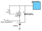
I have some difficulties to imagine the schematic:
dessin.png

How the gate changes his states low to high?


An ideal diode requires an active circuit that monitors the MOSFET voltage drop. Schottky rectifiers might be a suitable solution, too.
Do you have any schematic?

Hi,

We don´t know what the usual load current is.

But there are a lot of integrated circuits.
The benefit is the low voltage drop. Less than schottky rectifiers.
One manufacturer example: (There are many other manufacturers). Do a simple search on your own.
http://www.linear.com/parametric/PowerPath_Controllers_*_Ideal_Diodes

Klaus

Thanks for the link,
my low power µC needs few mA (<5mA) and inLow-power mode:
❐ Deep Sleep: 1.3 µA with watch crystal oscillator (WCO) on
❐ Hibernate: 150 nA with SRAM retention
❐ Stop: 60 nA with XRES wakeup

Thanks for the link,
what do you think about this one:
http://cds.linear.com/docs/en/datasheet/4417f.pdf

3 Inputs but the voltage range starts at 2.5V :s
 

Hi,

your schematic of post#8:
There is a mistake in the symbol. Correct it. (Either the body diode is in wrong direction or it is no P-Ch)

For sure the gate needs some logic to drive it. Currently there are just the powerpath switches.
Your uC maybe has an ADC to measure all the capacitor voltages... and four outputs for the Mosfet_gates.

There is no need to meausure with a high rate. Maybe once every 10s is enough.

Without any gate driven low the uC gets it´s power via the mosfet internal body diodes. There will be about 0.55V of voltage drop.
Adding schottky diodes in parallel to the internal body diodes may reduce the voltage drop.

***
Another question:
Why do you have four capacitors with individual charge levels? What is the idea behind this? Why not one big capacitor?

Klaus
 

Wow, now I'm completly confused.
Here is the right schematic:
schemeit-project.png

"Without any gate driven low the uC gets it´s power via the mosfet internal body diodes. There will be about 0.55V of voltage drop.
Adding schottky diodes in parallel to the internal body diodes may reduce the voltage drop. "
So what is the point of this circuit compare to a simple schottky diode if finnaly I still have a schottky diode with a low voltrage drop at the end?

Sorry I really don't understand, here is the schematic of what i think you tell me:
CommandPMOS (1).png

"For sure the gate needs some logic to drive it. Currently there are just the powerpath switches.
Your uC maybe has an ADC to measure all the capacitor voltages... and four outputs for the Mosfet_gates."
I need an ADC powered to drive the fourth PMOS, means I need minimum one PMOS to powersupply the ADC, it's like a loop ∞


"Why do you have four capacitors with individual charge levels? What is the idea behind this? Why not one big capacitor?"
Imagine that I have a solar cells which charge a super cap, another solar cell charges a super cap, a micro motor generator charges another supercap then micro motor generator charges a 4th supercap.
It's like energy havesting, I want to use these potential energy to supply a my µC

Thank you very much for your help I really appreciate
 

Hi,

So what is the point of this circuit compare to a simple schottky diode if finnaly I still have a schottky diode with a low voltrage drop at the end?

I said:
"Without any gate driven low the uC gets it´s power via the mosfet internal body diodes"
.. But when you drive the gte LOW, then it is very low impedance. --> almost no voltage drop.

****
I need an ADC powered to drive the fourth PMOS, means I need minimum one PMOS to powersupply the ADC, it's like a loop ∞
See above. The uC runs even if the gates are not driven. So the uC will start up in any case.
--> it´s not the "bad" loop that will prevent from start up, it is the "good" loop that lets you start up in any case.
Then you may use the software to select which capacitor to use.....
You or your software has the choice..

****
Honestly, it will be more efficient and more simple, if every source charges one common supercap.
The stored energy isn´t optimized if you have four independent capacitors.

My car has only one fuel tank. And not individual fuel tanks for different fuel brands.

Klaus
 

Hi,


I said:
"Without any gate driven low the uC gets it´s power via the mosfet internal body diodes"
.. But when you drive the gte LOW, then it is very low impedance. --> almost no voltage drop.

****

See above. The uC runs even if the gates are not driven. So the uC will start up in any case.
--> it´s not the "bad" loop that will prevent from start up, it is the "good" loop that lets you start up in any case.
Then you may use the software to select which capacitor to use.....
You or your software has the choice..

****
Honestly, it will be more efficient and more simple, if every source charges one common supercap.
The stored energy isn´t optimized if you have four independent capacitors.

My car has only one fuel tank. And not individual fuel tanks for different fuel brands.

Klaus

Hum thank you
I thought it would be possible to connect all my super cap together auto balanced and get a big tank of energy.
Like small rivers which drop in a big lac :)
But you are right, one big capa should be more optimized.
 

Status
Not open for further replies.

Similar threads

Part and Inventory Search

Welcome to EDABoard.com

Sponsor

Back
Top