Continue to Site

Welcome to EDAboard.com

Welcome to our site! EDAboard.com is an international Electronics Discussion Forum focused on EDA software, circuits, schematics, books, theory, papers, asic, pld, 8051, DSP, Network, RF, Analog Design, PCB, Service Manuals... and a whole lot more! To participate you need to register. Registration is free. Click here to register now.

Isolate Analog and Digital power Rails in ADC circuit

Status
Not open for further replies.

sps101

Newbie level 6
Joined
May 24, 2016
Messages
13
Helped
0
Reputation
0
Reaction score
0
Trophy points
1
Activity points
127
I am designing an ADC in umc 65nm which operates at 1GHz. The analog section consists of the sample and hold and a bunch of comparators. The digital section consists of an Encoder(synthesized in Cadence Encounter).
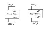
When I connect the analog section and digital section to different power rails(VDD_A and GND_A for analog section and VDD_D and GND_D for digital section) I get an LVS error saying that there is a stamping error.
But when I connect both sections to the same ground the LVS passes.
The LVS error I get is
LVS error isolated grounds.JPG
 

maybe this can be waivered. check with the foundry. the PDK might mention some extra steps you have to take care of to label these special nets.
 

maybe this can be waivered. check with the foundry. the PDK might mention some extra steps you have to take care of to label these special nets.

Thank you for the mail. I will try to do that.
Maybe a cause of this might be because the digital encoder is designed using the standard cells which has the substrate tied to global VSS and VDD. When I integrate the analog section with the digital section, the different biasing of the analog substrate and encoder substrate is causing the conflict.

I am thinking of connecting only the body terminals of the transistors in the analog section to the same potential as that of the digital encoder VDD and VSS and just keeping the analog section's power and ground rails different(VDD_A and GND_A).

My concern is that since the digital power rails are quite noisy, would this affect the transistors in the analog section(body effect) due to the same substrate connection ?

- - - Updated - - -

Just to make my previous post clearer. The below configuration gives the LVS stamping conflict error
LVS stamping conflict error.JPG

This configuration has no LVS error but I am concerned if the noise of the digital ground will impact the performance of the analog blocks through the substrate.
VBN same potential as GND_D no LVS error.JPG
 

Status
Not open for further replies.

Part and Inventory Search

Welcome to EDABoard.com

Sponsor

Back
Top