Continue to Site

Welcome to EDAboard.com

Welcome to our site! EDAboard.com is an international Electronics Discussion Forum focused on EDA software, circuits, schematics, books, theory, papers, asic, pld, 8051, DSP, Network, RF, Analog Design, PCB, Service Manuals... and a whole lot more! To participate you need to register. Registration is free. Click here to register now.

[Moved]: Regulator Ripple rejection

Status
Not open for further replies.

tiwari.sachin

Full Member level 6
Joined
Aug 1, 2009
Messages
341
Helped
3
Reputation
6
Reaction score
3
Trophy points
1,298
Location
India
Activity points
4,449
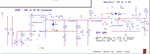
I am using a DC to DC buck to convert 24V to 5V

Followed by that a LM1117 to convert 5V to 3.3V

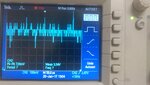
Although I am getting the required 5V and 3.3V but I see a lot of noise (ripples) at the output.

I am using 47uF Ceremic caps at 5V

and 10uF Ceramic caps with series 1R resistor at output of 3.3V


I did try to have more parallel caps but its not effecting much.

Any suggestions for how I can possibly reduce these ripples

- - - Updated - - -

The DC to DC operates at Fixed 570 kHz Switching Frequency
 

Re: Regulator Ripple rejection

Any schematic...How can i we say anything without much data. Any captures you took etc..
 

Re: Regulator Ripple rejection

11.jpg

This is how my schematic is
 

Re: Regulator Ripple rejection

5V AND 3.3V waveforms are as follows

5V.jpg

**broken link removed**

- - - Updated - - -

I want to make the output constant... 10-20mV should be acceptable but what variations i am getting is way too much
 

Attachments

  • 3V3.jpg
    3V3.jpg
    506.2 KB · Views: 80

Re: Regulator Ripple rejection

Do you measure the same noise on the output of the switcher (TP5) that you see on the linear regulator output?
 

Re: Regulator Ripple rejection

LM117 is too slow to be an effective filter for 100kHz
range (or higher) DC-DC converter ripple (which has
strong harmonics extending up a few decades from
baseband). Its high frequency PSRR is poor (should
be able to see this in the datasheet characteristic
plots or some app notes). This means that any AC
content has to be knocked down by other means.
If you have the space and headroom, a LC filter
before the LM117 and let the regulator make up for
the DC resistance and any lower frequency transient
response (like load step) issues. This latter says
more (and better) C and less L, in the filter.

Now in the vein of "better C", adding a semi-infinite
amount of ineffective capacitors does nothing but
cost money. Your capacitor selection for DC-DC output
(and input) filter needs to comprehend ESL and ESR.
These make a filter lose effectiveness above the
1/(ESR*C), 1/sqrt(ESL*C) corner frequencies. At
100kHz and above electrolytics and many tantalums
become ineffective and only high quality ceramics
can cut the head off the HF ripple (and this is still a
matter of degree, there is no "brick wall filter" in real
power PCB design, unlike simple SPICE circuits). You
should (if interested) find the lumped element models
for the caps you have now, and replace any design
generic components with parasitics aware ones. This
may be enlightening (especially if you can push PCB
and chip parasitics into the mix as well, make a
realistic ground-mesh and so on - but this is the kind
of thing that can go on for a while and you'd like to
do on somebody else's dime).

There are better LDOs meant exactly for this
application that optimize HF PSRR. Liear Tech for
sure, probably TI, probably some others.

Now if your switcher shares the same ground,
you need to be sure that what you measure is
real as the "client" sees it. DC-DC switching
always contaminates the ground and the 'scope
doesn't know from nuthin', about what noise is
ground bounce against a quiet DC voltage, or
what's regulated voltage noise against a quiet
ground. One quick thing to try is leave the ground
clip where it is, and measure a ground point close
to where you're taking your ripple measurement
now (as shown). You may see the same hash on
ground #2 as on Vreg. In which case you need to
tighten up your measurements, maybe impose a
common mode choke (module?), and so on. EMI
characterization and exorcising those demons is
a black art all its own. You may have to sacrifice
your first-born (PCB layout) to appease them.
 
Last edited:
  • Like
Reactions: Salvu

    Salvu

    Points: 2
    Helpful Answer Positive Rating
Re: Regulator Ripple rejection

Agree with the comment about probably incorrect measurement. Even a LDO with poor high frequency rejection would have considerably lower output ripple if the ceramic output capacitors are actually in place and effective.
 

Re: Regulator Ripple rejection

The LM117 data sheet shows good ripple rejection out to about 10kHz as shown below., which appears to be the ripple frequency of your converter, so the ripple out of the LM117 should be significantly reduced.
Note that adding a capacitor from the ADJ terminal to ground substantially increases the ripple rejection.

Otherwise you likely have a bad ground layout.
Switching regulators require a ground plane if you need low noise.


Capture.PNG
 

Re: Regulator Ripple rejection

This is how the board layout is

1.png

2.png

BOTTOM LAYER.png

TOP_LAYER.png

- - - Updated - - -

The area for power design 5V and 3.3V is 35x18mm approx

- - - Updated - - -

3.png

GND Layer along with stackup details (can be seen on the right)

- - - Updated - - -

As referred by dick_freebird, I have a flat common GND beneth components placed (ie power components on TOP and very next layer is GND)

- - - Updated - - -

I am planning to go with another board with 5V (DC to DC Buck on TOP LAYER
and 1117 Regulator (Ofcourse input if 5V from Buck) at BOTTOM LAYER.

What precautions are suggested with routing for scenario like this.

I wont place 1117 exactly below buck though (Never)
 

Re: Regulator Ripple rejection

I see a weakness in the ground wiring of switcher input and output filter capacitors, although I have problems to indentify the vias connecting to the ground plane.

You are apparently trying to implement a locale power ground on top layer and connect filter capacitors not directly to ground plane. This can be an effective means to keep commutating currents in the locale ground and avoid spilling it allover the ground plane. But it should be supplemented by LC filters shorting the ripple voltage to the ground plane. E.g. C5- should be connected directly to ground plane and an inductor or high current ferrite bead between C10/C11+ (switcher output node) and C5+. The switcher 24V input with it's discontinuous current is even more critical should get similar filtering.
 

Re: Regulator Ripple rejection

I posted the ripple rejection for the 117 instead of the 1117 (below), but they are similar.

Capture.PNG
 

Re: Regulator Ripple rejection

FVM. I already have a 10uH inductor.

- - - Updated - - -

SCH.png

This is how you are suggesting me to use??
 

Re: Regulator Ripple rejection

Hi,

In your design there are some LC filters.
I (personally) don´t like those high Q LC filters, because of their resonance.
Usually when I use then, then I add some damping circuit, usually an RC.
With given component values you easily can claculate reosnance frequency of an LC, then add an RC that dissipates some power at this resosnance frequency.
This helps to avoide resonance / ringing.

***
The 1117 has some problems with very low ESR. So you need to add a resistor.
Now you added them in seires with the capacitor, but also in parallel with the load.
For sure this resistance now decreases the attenuation of high frequencies.

You can try this instead:
1117 output -> 33mOhms series R -> Capacitor -> GND
Connect the load parallel to the capacitor.

The drawback is that every load current will cause a voltage drop in this resistor.

****
But I still think about a measurement problem.
Induced noise...
or common mode noise that causes current to flow in the scope porobe´s GND line...

Klaus
 

Re: Regulator Ripple rejection

I already have a 10uH inductor.
That's the regular buck converter inductor.

As for the circuit with ferrite filters, the ground layout definitely matters.

See below an example of a DC/DC converter (buck-boost in this case) with local power ground, star point connector to global ground and filters.

dcdc_filter.jpg

LC filters can involve in fact unwanted oscillating load step responses, you need to check the quality factor set by the filter and load impedance. I see acceptable behavior with capacitors in the 10 µF range and ferrite beads.
 

Re: Regulator Ripple rejection

An RC snubbed across the LM1117 (i.e. from input to output) will improve its output ripple.


--Akanimo.

- - - Updated - - -

An RC snubbed across the LM1117 (i.e. from input to output) will improve its output ripple.

It should help you reduce the capacitance that you need at the output/GND.

--Akanimo.
 

Re: Regulator Ripple rejection

Do you measure the same noise on the output of the switcher (TP5) that you see on the linear regulator output?

As seen in the waveforms, the output of buck variation is less compared to that of regulator
 

Re: Regulator Ripple rejection

An RC snubbed across the LM1117 (i.e. from input to output) will improve its output ripple.
How? LM1117 needs output capacitors with high ESR for stability, they can be considered as RC snubbers or lossy bypass capacitor. A RC snubber between input and output can be expected to form a voltage divider with the output filter and reduce ripple rejection.

- - - Updated - - -

As seen in the waveforms, the output of buck variation is less compared to that of regulator
I won't overrate the measurement results. This may be the result of an unsuitable ground connection.

Or LM1117 is marginal stable with the present output capacitor dimensioning and actually increasing the output ripple. If so, the regulator bypassing should be corrected, or a ceramic-C stable regulator used.
 

Re: Regulator Ripple rejection

How? LM1117 needs output capacitors with high ESR for stability, they can be considered as RC snubbers or lossy bypass capacitor. A RC snubber between input and output can be expected to form a voltage divider with the output filter and reduce ripple rejection.

The ripple could be a result of an unsuitable ground connection though, but since connecting an RC snubber (LM1117.IN --> 1ohm<R<2ohm --> C --> LM1117.OUT) can reduce the ripple, and it can, it is worthwhile trying it out.

Try out capacitors in order of uF to 10s of uF. It should work.
 

Re: Regulator Ripple rejection

I have added a boot resistor (Not given in datasheet though)

R C Series at output of Buck

R - C Series at LM1117 input and output

and as KLausST suggested R-C at output to ground

Added ferrite at the output of 1117

SCH2.png

Updated Sch...

1. Is it right that I am doing??

2. Are the ferrite parts that I have chosen suitable.

Designed Bulk considering max current output 0f 2.5A
 

Attachments

  • SCH2.png
    SCH2.png
    43.6 KB · Views: 74

Re: Regulator Ripple rejection

Without going into a very deep analysis, I believe that R9/C15 are in the wrong location.

They are between the switching node and ground. At your 570 Khz frequency, the capacitor is essentially a short (well, it does have ESR) in series with a 1 ohm resistor.

That snubber circuit should be located across L1, and its time constant should be high enough to suppress the ringing frequency only. You are talking a capacitor in the picofarad range.
 

Status
Not open for further replies.

Similar threads

Part and Inventory Search

Welcome to EDABoard.com

Sponsor

Back
Top