Continue to Site

Welcome to EDAboard.com

Welcome to our site! EDAboard.com is an international Electronics Discussion Forum focused on EDA software, circuits, schematics, books, theory, papers, asic, pld, 8051, DSP, Network, RF, Analog Design, PCB, Service Manuals... and a whole lot more! To participate you need to register. Registration is free. Click here to register now.

voltage regulator not working

Status
Not open for further replies.

gauravkothari23

Advanced Member level 2
Joined
Mar 21, 2015
Messages
640
Helped
5
Reputation
10
Reaction score
4
Trophy points
1,298
Activity points
6,922
hi all...
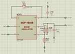
i am trying to build a boost regulator to get a output of 5V with input voltage from li-po battery (3.2v to 4.2v) using MCP1640B (6 pin sot23).
but the output voltage i am getting is as equal to the input voltage.
as per the datasheet the resistor to be used at FB pin should be 976K and 309K. but 976K resistor is not easily available in the market so i am using 510K and 470K resistor in series.
can anybody please help me to resolve the issue.
circuit diagram attached.
 

Attachments

  • MCP1640B.png
    MCP1640B.png
    26.9 KB · Views: 92

The FB pin compared to internal 1.21V reference. Recalculate your devider with more suitable values yourself, you can do that.
E24_Calc.PNG
 
Last edited:

It is not the problem with resistor divider. Try this for crosschecking
1) You should get 3.6V if you put all three resistors value 470KΩ
2) You should get 6V when 470KΩ series on top side and 470KΩseries on bottom side

Please check the DC resistance of the resistor by multimeter!!!!!!!!!!!!
Check the inductance value in LCRR meter
 

as per the datasheet....
i think its not an issue of voltage divider resistor values
MCP1640B12.pngMCP1640B1.png

- - - Updated - - -

It is not the problem with resistor divider. Try this for crosschecking
1) You should get 3.6V if you put all three resistors value 470KΩ
2) You should get 6V when 470KΩ series on top side and 470KΩseries on bottom side

Please check the DC resistance of the resistor by multimeter!!!!!!!!!!!!
Check the inductance value in LCRR meter

under all the conditions, i am getting vout @ 3.05V

- - - Updated - - -

i have also checked the resistance of a resistor 470K.. it shows a proper value but when the same resistor is soldered to the PCB, it shows 234K.. how is it possible.
 

Hi,

Your output voltage makes me think it is not switching.

What is your EN connection?


Show us your PCB layout.
This circuit is not suitable to test on a breadboard.

Klaus
 

the EN connection is connected to vin.
but why do the resistance value of a resistor changes when after soldered to the PCB. 470K value resistor near about 234K
 

under all the conditions, i am getting vout @ 3.05V
Means the boost is off all time. EN is shown as a separate port in your schematic, not tied to VIN. Is it activated at all?


i have also checked the resistance of a resistor 470K.. it shows a proper value but when the same resistor is soldered to the PCB, it shows 234K.. how is it possible.
Simply expectable. It's impossible to measure resistors in circuit without special requisites (and profound knowledge how-to), just forget about it.

Measuring Vfb with a high impedance multimeter (Rin >= 10 Mohm) seems the most simple way to check for correct voltage divider operation. If the boost converter is deactivated by incorrect voltage divider, Vfb would be near to or above 1.2V With correct divider, you'll see below 1.2V with 3 or 4V Vout.

- - - Updated - - -

You should also check all device terminal voltages for plausibility.

If EN is activated and the 4.7 µH inductor is a suitable device, other possible explanations for failure are:
- soldering fault
- wrong pin order
- boost converter damaged
 

You should also check all device terminal voltages for plausibility.

If EN is activated and the 4.7 µH inductor is a suitable device, other possible explanations for failure are:
- soldering fault
- wrong pin order
- boost converter damaged

I have checked that the voltage regulator gets extremely hot. is it due to wrong pin order

- - - Updated - - -

but i have checked the pin indication marking with white dot on the IC, which indicates PIN 1
 

Can you show a circuit photo?
attaching the circuit..
sorry but the things are bit messed up...

- - - Updated - - -

i have even tried changing the regulator... but the problem continues...
the regulator gets hot when the circuit is on..
 

Attachments

  • IMG_20170104_172511.jpg
    IMG_20170104_172511.jpg
    499.8 KB · Views: 94

I had same issue long time ago. EN pin have to be connected through 1-100k resistor.
 

But why do the regulator gets hot and that too within a second.
 

I wonder where the output capacitor is placed?

I believe the layout is far from fulfilling this datasheet requirement:
3.2 Ground Pin (GND)
The ground or return pin is used for circuit ground connection. Length of trace from input cap return, output cap return, and GND pin should be made as short as possible to minimize noise on the GND pin.
 

I wonder where the output capacitor is placed?

I believe the layout is far from fulfilling this datasheet requirement:
agreed with you...
but can this be the reason for regulator to get hot
 

MCP1640.jpg

Please check the track, i found one fault connection in the PCB
 

The bad ground connection can cause all kinds of problems, even serious overvoltage that may damage the device. Also placing the output capacitor not near to the switcher can cause similar problems.

I would try to arrange the components similar to datasheet figure 5.1.

There may be also more trivial reasons for a damaged device. E.g. if it has been operated inadvertently with open feedback loop or without output capacitor.
 

MCP1640-1.jpg
Pin no 6 and pin no 3 should be short
Not able to understand the ground connection
 

The ground connection is "understandable" but really bad.
EN is apparently connected externally, at least the OP claimed this. If not enabled, the converter would stay off and surely not run hot.

- - - Updated - - -

Another point. I'm unable to recognize expected MCP1640B package marking "BWNN". Instead I see "BW3K" or similar. Sure it's the right device?
 

Hi,

I recommend to re-read the whole datasheet, maybe additional informations about SMPS.

Output capacitor:
Energy is stored in the inductance when the IC internal Mosfet switches to GND.
--> now the current loop is:
* from input capacitor
* through inductor
* through IC to GND
* and back to the input caoacitor.
This whole loop needs to be short, thick traces and should enclose only a small area.
..
Then the switch releases and the whole stored energy is pushed into the output capacitor.
The stored energy in the inductor is: I x I x L x 0.5
The stored energy in a capacitor is: U x U x C x 0.5
Imagine a fixed value of energy is stored in a capacitor, then this means: the smaller the capacitor, the higher the voltage.
no (output) capacitor --> unpredictable high voltage
This may immediately kill the IC.

The current loop for an open switch is:
* input capacitor
* inductor
* catch diode or active rectifier mosfet (here inside IC)
* output capacitor
* back to input capacitor via GND
This whole loop needs to be short, thick traces and should enclose only a small area.

Klaus
 

Status
Not open for further replies.

Part and Inventory Search

Welcome to EDABoard.com

Sponsor

Back
Top