Continue to Site

Welcome to EDAboard.com

Welcome to our site! EDAboard.com is an international Electronics Discussion Forum focused on EDA software, circuits, schematics, books, theory, papers, asic, pld, 8051, DSP, Network, RF, Analog Design, PCB, Service Manuals... and a whole lot more! To participate you need to register. Registration is free. Click here to register now.

Question of building a class E power amplifier in driving the wireless power coil

Status
Not open for further replies.

bhl777

Full Member level 6
Joined
Sep 30, 2008
Messages
363
Helped
0
Reputation
0
Reaction score
0
Trophy points
1,296
Activity points
5,140
Hi All, I am new to PA and building a class E PA in driving the wireless power coil. Currently I can get the sinusoidal waveform at the coil, but it is still not functional. Would any one help me point out the problems I have?
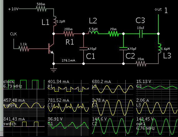
This is my schematic.
PA.png
The switching frequency is 6.78MHz. I am using the switch F12N10L,C2=33pF, L2=4.2Uh(Wurth 744325420), C3=100pF, L3 is 7.8uH (Wurth 760308103307), L1 is a large one but it seems it does not play a critical role. I am using a fucntion generator to go through a digital AND gata to drive the FET.
During my test, no secondary WPT coil is placed around. So ideally I suppose this should be like a "no load" condition. However, there are many problems of my exsiting circuits:
(1) the switching node looks wired
(2) at this no load condition, I_VDD is very high
(3) as VDD increases, the peak to peak amplitdue of Vcoil goes up first then goes down. For example, I want to have a 15V Vpeak to peak amplitude of the Vcoil, but I can never get it using the exsiting circuit.
PA1.png
PA2.png
PA3.png
Would any one tell me what makes this PA not functional? The perfect resonance is not necessary, but I do want to have a tunable peak to peak amplitude of the Vcoil, that I can use to transfer to the secondary coil. Thank you!
 

Look for a faster transistor which still meets your requirements.
The gate shows a bit of ringing, some resistance in series with the gate will lower it a bit, but the drawback is that it makes transistor slower.
 
Last edited:

Did you try to tune the series resonant circuit?

Yes I did try to change the L2 value and C3 value, but it did not help too much. I am not sure which component is the key to get I want. The first thing I want to get is a higher peak to peak amplitue of the Vcoil, because I will use a secondary coil to get a 1:1 AC signal then rectified it to a DC level. Thank you!

- - - Updated - - -

Look for a faster transistor which still meets your requirements.
The gate shows a bit of ringing, some resistance in series with the gate will lower it a bit, but the drawback is that it makes transistor slower.

Hi CataM, do you think the transistor is the key in making the wired waveform in switching node? I do not have other transistors available at this moment, but if that can solve my problem, I will add a series resistor to the gate.
 

Yes I did try to change the L2 value and C3 value, but it did not help too much. I am not sure which component is the key to get I want.
I suggest to read about class E's principle of operation and its design equation e.g. "Generalized Design Equations for Class-E Power Amplifiers with Finite DC Feed Inductance" from IEEE.
I would kindly give that paper to you but forum rules does not allow it. Anyway, it should not be hard to find it.

Hi CataM, do you think the transistor is the key in making the wired waveform in switching node? I do not have other transistors available at this moment, but if that can solve my problem, I will add a series resistor to the gate.
You have to keep in mind that in practice nothing is ideal, including your 0.2 ohm Rds(on) which may keep you away from achieving what you want.
Obviously the closer to ideal operation of the circuit, better will perform. I do not think 100% that the ringning in the gate can solve anything, but a faster transistor yes since this is a ZVS operating circuit.
 

I suggest to read about class E's principle of operation and its design equation e.g. "Generalized Design Equations for Class-E Power Amplifiers with Finite DC Feed Inductance" from IEEE.
I would kindly give that paper to you but forum rules does not allow it. Anyway, it should not be hard to find it.


You have to keep in mind that in practice nothing is ideal, including your 0.2 ohm Rds(on) which may keep you away from achieving what you want.
Obviously the closer to ideal operation of the circuit, better will perform. I do not think 100% that the ringning in the gate can solve anything, but a faster transistor yes since this is a ZVS operating circuit.

Thank you CataM. I only have a few FET to select at this moment. Would you tell me which parameter I should check in the FET datasheet to see if it is a faster transistor? Thank you!
 

C2=33pF, L2=4.2Uh
C3=100pF, L3 is 7.8uH

Current is restricted to a small level by your small C values. You need an L:C ratio which is associated with greater current levels. This will give you more current going through the coil. That is what you really want, isn't it?

There are other LC oscillators which might work better for you. Consider this one.

The long-tail pair automatically senses the resonant frequency of the LC tank. It provides an energy 'kick' at the right time in the cycle. Sine-shaped oscillations build and sustain.
(I built a hardware version and it works. Mine was low current and low frequency.)

3784081100_1482212468.png


Notice peaks of 1/2 A going through the coil. Supply voltage is about 4V. I included a fraction of an ohm resistance in the coil (in an effort toward realism in simulation). Less than 1/10 A is required from the supply.

To adjust output level, change supply voltage, or adjust resistor R.

I want to have a 15V Vpeak to peak amplitude of the Vcoil, but I can never get it using the exsiting circuit.

It is possible to get voltage swings of much greater amplitude than the supply voltage. Select a very large L:C ratio (capacitor value very small in relation to the inductor). However the large amplitude does not guarantee you have a lot of current going through the coil. Furthermore the sinewave may become distorted. It's the capacitor playing a dominant role in setting the current level. It sets it very low. In turn the inductor creates higher voltage levels. I saw it with my own eyes. Waveforms at 20V amplitude when the supply is only 5V.
 

Hi BradtheRad, thank you so much for your advice! Currently my problem is coming from the current capability. For some reason I have to use class E PA instead of your LC oscillator. Would you advise me what should I change for my current PA?

Right now I have modified the board a little bit, according to the structure in this paper: **broken link removed**. I am using the L,C components with closest values to that structure.

This is the schismatic of my board, and my target is to maintain the rectified voltage at the secondary coil higher than 5.5V when max load =100mA.
PA.png

At no load condition, I am able to get the rectified voltage higher than 10V, when VDD is only around 3V and the I_VDD=0.25A. However, there is no sourcing capability of the rectified voltage. When I placed a 100ohm resistor load at the Vrect, it went down to 3.XXV, and cannot go up to this level, even if I increase VDD. I did try to change C3 value from 10nF to 100pF, but that does not help in boosting the current sourcing capability. Would you advise me what should I change in this structure to achieve my goal?

Thank you so much!


Current is restricted to a small level by your small C values. You need an L:C ratio which is associated with greater current levels. This will give you more current going through the coil. That is what you really want, isn't it?

There are other LC oscillators which might work better for you. Consider this one.

The long-tail pair automatically senses the resonant frequency of the LC tank. It provides an energy 'kick' at the right time in the cycle. Sine-shaped oscillations build and sustain.
(I built a hardware version and it works. Mine was low current and low frequency.)

3784081100_1482212468.png


Notice peaks of 1/2 A going through the coil. Supply voltage is about 4V. I included a fraction of an ohm resistance in the coil (in an effort toward realism in simulation). Less than 1/10 A is required from the supply.

To adjust output level, change supply voltage, or adjust resistor R.


It is possible to get voltage swings of much greater amplitude than the supply voltage. Select a very large L:C ratio (capacitor value very small in relation to the inductor). However the large amplitude does not guarantee you have a lot of current going through the coil. Furthermore the sinewave may become distorted. It's the capacitor playing a dominant role in setting the current level. It sets it very low. In turn the inductor creates higher voltage levels. I saw it with my own eyes. Waveforms at 20V amplitude when the supply is only 5V.

- - - Updated - - -

I suggest to read about class E's principle of operation and its design equation e.g. "Generalized Design Equations for Class-E Power Amplifiers with Finite DC Feed Inductance" from IEEE.
I would kindly give that paper to you but forum rules does not allow it. Anyway, it should not be hard to find it.


You have to keep in mind that in practice nothing is ideal, including your 0.2 ohm Rds(on) which may keep you away from achieving what you want.
Obviously the closer to ideal operation of the circuit, better will perform. I do not think 100% that the ringning in the gate can solve anything, but a faster transistor yes since this is a ZVS operating circuit.

Hi CataM, I followed the procedure shown in the paper in designing the PA, but it seems that does not work. I am using X=1.6uH and R=100 Ohm, (my load is the coil, so according to the paper, I need to put the 100Ohm in satisfy the equations). However, using L0=16uH,C0=33pF, L=6mH, C=33pF, I am still not able to get the target peak to peak amplitude of the Vcoil. Therefore, I am not able to move ahead to put my secondary coil in. I also tried in putting a 10 Ohm series resistor in that gate of the FET, but that does not help too much. Would you give me some more suggestions?
 

L1 is a large one but it seems it does not play a critical role

This is the inductor near the supply V+. I believe it acts the same as a boost converter.

(1) First it is grounded by the mosfet for a while.
(2) Current builds to 1A or more.
(2) The mosfet shuts off.
(3) Inductive kick sends a jolt of current into the righthand portion of your circuit. (The supply voltage is added to the emf.)
(4) The combined components ring for a few cycles (6.8 MHz), at high amplitude (20 or 30 or 40V).

If I have the correct idea, then the above sequence sends a few cycles at high voltage to the transmitting coil, then it waits a while. (So perhaps it is not designed to generate a sinewave continuously? My post #7 schematic generates a continuous sinewave.)

Questions that arise:

* Does the paper instruct to drive the mosfet at 7MHz, or at a lower frequency, say, less than 1 MHz?

* What results do you get when you increase the value of L1 (the inductor closest to supply +)? When you increase it to 1 uH?
 

Hi BradtheRad, thank you for your help. My target is to generate a continuous sinewave. But the procedure in that paper did not mention the range of frequency it can support.
Here is what I found:
1. On my first prototype board before I used the menthod in that paper, I changed L1 from 1uH to tens of uH. Current always built to 1A or more, the peak to peak Vcoil never can go above ~6V, no matter what VDD is.
2. On my second prototype board after I used the menthod in that paper, by calculation L1 should be 6mH (milli henry), with a sereis 100 Ohm resistor with the coil. I tried several values of L1, the current is now only 0.2A when I have only the primary wireless coil being driven (I guess it is much more like ZVS than the first prototype). However, the peak to peak Vcoil never can go above ~6V, no matter what VDD is.
3. On my third prototype board, I used the values closest to the ones presented in **broken link removed**. As I mentioned to you in the previous thread, at no load condition, I am able to get the rectified voltage higher than 10V, when VDD is around 3V and the I_VDD=0.25A. However, there is no sourcing capability of the rectified voltage. One thing I am not sure on this board is the high Q inductor. In this paper, it said the inductor of L-type matching network should be with high Q. However, I did not find the Q information from the inductor I was used. It is a 1.5uH inductor that can support 15A DC current, which was used for buck converter.

Would you give me some more instruction how can I solve my problem? It seems like fixing the current sourcing capability / increasing the maximum power of my third prototype board could be the quickest solution. In addition, would you tell me if you think the Q of the inductor in my 3rd prototype board could be an issue in causing the sourcing capability? Thank you!

This is the inductor near the supply V+. I believe it acts the same as a boost converter.

(1) First it is grounded by the mosfet for a while.
(2) Current builds to 1A or more.
(2) The mosfet shuts off.
(3) Inductive kick sends a jolt of current into the righthand portion of your circuit. (The supply voltage is added to the emf.)
(4) The combined components ring for a few cycles (6.8 MHz), at high amplitude (20 or 30 or 40V).

If I have the correct idea, then the above sequence sends a few cycles at high voltage to the transmitting coil, then it waits a while. (So perhaps it is not designed to generate a sinewave continuously? My post #7 schematic generates a continuous sinewave.)

Questions that arise:

* Does the paper instruct to drive the mosfet at 7MHz, or at a lower frequency, say, less than 1 MHz?

* What results do you get when you increase the value of L1 (the inductor closest to supply +)? When you increase it to 1 uH?
 

Would you tell me which parameter I should check in the FET datasheet to see if it is a faster transistor?
Look the delay time and fall time. Total on time is delay + rise time. To see if it is faster, just look to the delay time.
However, I think this should be done at the very end after the circuit is matched perfectly... and your circuit is not very slow, comparing ns to the switching frequency, so the faster transistor can wait.

One thing I am not sure on this board is the high Q inductor. In this paper, it said the inductor of L-type matching network should be with high Q. However, I did not find the Q information from the inductor I was used. It is a 1.5uH inductor that can support 15A DC current, which was used for buck converter.
In your paper they said they used inductors with Q=120 if I recall.
Q of coil can be calculated by ωL/ESR with ESR = DC resistance of the coil.
For the chocke, use a magnetic core for it, not with air core like the Tx coil.
 

Hi CataM, thank you so much for your help! Yes, from that paper a Q=120 is used for the matching netwrok.

Both inductors I am using have similar packaging like this: https://katalog.we-online.de/pbs/datasheet/7443330470.pdf , is there any problems? I guess they are not RF chokes.
The typical DCR of that 1.5uH inductor is around 0.04 Ohm, so according to your equation, at 6.78MHz, Q is aroun 1600, which is much higher than the one with Q=120 in the paper. Should I expect a better performance of the system with this inductor with a higher Q? Or is there any potential problems?

Currently I have a much reduced I_VDD, which means using this configuration, it is much more like the ZVS during the operation. However, the rectifid voltage cannot source the current I want (up to 100mA). I think the cause is still coming from the class E PA, but am not sure how can I enhance the power level. Increasing VDD is not useful. Do you have some more suggestions?

Thank you!

Look the delay time and fall time. Total on time is delay + rise time. To see if it is faster, just look to the delay time.
However, I think this should be done at the very end after the circuit is matched perfectly... and your circuit is not very slow, comparing ns to the switching frequency, so the faster transistor can wait.


In your paper they said they used inductors with Q=120 if I recall.
Q of coil can be calculated by ωL/ESR with ESR = DC resistance of the coil.
For the chocke, use a magnetic core for it, not with air core like the Tx coil.

- - - Updated - - -

Hi CataM, I have another question. Is it possible that the sourcing capability of the secondary coil related to the rectifier circuit? For example, in this 6.78MHz class E PA, https://aaronscher.com/Circuit_a_Day/Single_diode_rectifiers/rectifier_images/2015-rectifierTPEL.pdf , a class E rectifier at the secondary coil is used to generated the rough DC voltage.
rectifier.JPG

What I have now is only a full bridge rectifier (https://www.infineon.com/dgdl/bas40...c04c4&fileId=db3a304329a0f6ee0129a6dc9f802b68), is it possible if I build a class E rectifier to boost the power capability?
Thank you!


Look the delay time and fall time. Total on time is delay + rise time. To see if it is faster, just look to the delay time.
However, I think this should be done at the very end after the circuit is matched perfectly... and your circuit is not very slow, comparing ns to the switching frequency, so the faster transistor can wait.


In your paper they said they used inductors with Q=120 if I recall.
Q of coil can be calculated by ωL/ESR with ESR = DC resistance of the coil.
For the chocke, use a magnetic core for it, not with air core like the Tx coil.
 

Going with your schematic in post #8, the single biggest improvement is to increase your center inductor to 5.5 uH. My simulation gets peaks over 2A in the transmitting coil.


Two loops act in resonance (at 6.8 MHz)... C1-C2-L2 & C2-C3-L3. One goes clockwise while the other goes counter-clockwise, then they switch directions.

Notice volt levels over 100V (theoretically, that is).

One thing I am not sure on this board is the high Q inductor. In this paper, it said the inductor of L-type matching network should be with high Q. However, I did not find the Q information from the inductor I was used.

As a general rules you can get high Q by minimizing ohmic resistance in components. My inductor models have a small ohmic resistance inline. If your real components have less resistance then your transmitting coil may reach greater power levels.

Possibly a tiny core of metal improves performance? A core concentrates magnetic flux within the inductor, and reduces interference between inductors which are located nearby.
 

Going with your schematic in post #8, the single biggest improvement is to increase your center inductor to 5.5 uH. My simulation gets peaks over 2A in the transmitting coil.


Two loops act in resonance (at 6.8 MHz)... C1-C2-L2 & C2-C3-L3. One goes clockwise while the other goes counter-clockwise, then they switch directions.

Notice volt levels over 100V (theoretically, that is).


As a general rules you can get high Q by minimizing ohmic resistance in components. My inductor models have a small ohmic resistance inline. If your real components have less resistance then your transmitting coil may reach greater power levels.

Possibly a tiny core of metal improves performance? A core concentrates magnetic flux within the inductor, and reduces interference between inductors which are located nearby.

Thank you BradtheRad! I will try you method and let you know how it goes. The only remaining question I have is about the peak volt levels (over 100V). In my case, my rectifier can only support 40V and secondary coil has a 1:1 ratio of the primary coil. In case I need to reduce the peak voltage level, do we have any simple solution (such as adding a R/C)?
 

In case I need to reduce the peak voltage level, do we have any simple solution (such as adding a R/C)?

The obvious things to try, is reduce supply V, or reduce bias to the transistor/ mosfet. Start small and ramp up to your intended power level.

Also be mindful about the Ampere level going through components. Who can say whether a little 470pF capacitor can endure, when it has 2A going back and forth through it 7 million times a second? And what volt rating do yours have? 50V is typical for small ceramics.

It's a good idea to monitor heat. And put a protective cover over your circuit, in case something explodes.
 
  • Like
Reactions: bhl777

    bhl777

    Points: 2
    Helpful Answer Positive Rating
What I have now is only a full bridge rectifier (https://www.infineon.com/dgdl/bas4002...29a6dc9f802b68), is it possible if I build a class E rectifier to boost the power capability?
Obviously Class E rectifier boosts efficiency, but is it needed ? Can you afford a bulkier and more expensive design? That bad is your bridge rectifier ?
Maybe you should check efficiency of your circuit and see where the problem realy is (efficiency of the class E PA, inductive link, rectifier).

Another thing is the heat in your semiconductor. How is the transistor ? Check if needs a heat sink and as for the heat on the passive devices Brad mentions, maybe is a good idea to divide the heat into several components e.g. 2 or more capacitors in paralel so that each carries less current and hence less heat. But... then you may have problems with tolerances of capacitors as they generally are not very good.
 
  • Like
Reactions: bhl777

    bhl777

    Points: 2
    Helpful Answer Positive Rating
The output capacitance Coss of your FET is far too high to work effectively at 6.78MHz. By a factor of ten at least. No improvement to the Q of your inductors or capacitors is going to make this circuit function well.

You need to either select a much more optimal FET, or decrease your operating frequency greatly.
 
  • Like
Reactions: CataM

    CataM

    Points: 2
    Helpful Answer Positive Rating
The output capacitance Coss of your FET is far too high to work effectively at 6.78MHz. By a factor of ten at least. No improvement to the Q of your inductors or capacitors is going to make this circuit function well.

You need to either select a much more optimal FET, or decrease your operating frequency greatly.

Hi mtwieg, thank you! Would you advise me the following questions?
(1) the COSS of F12N10L is 325pF, so you think using this FET can make my board not functional at all? Acutually I have to operate at 6.78MHz but I do not care about the efficiency. As far as it is functional, it is good enough for me.
(2) Now I have a 470pF in parallel with D and S terminals. Do you think reducing it will help?
(3) If you think COSS is the cause of my circuit, I suppose I need to look for a FET with around 30pF COSS?
(4) In addition to this, what other parasitic parameters I should pay attention to make sure the FET is suitable for the swicthing of this frequency? I do not know too much about power FET.
Thank you!
 

(1) the COSS of F12N10L is 325pF, so you think using this FET can make my board not functional at all?
Actually it's much higher than 325pF. Coss is a nonlinear function of Vds. At your low bias Vds, you will effectively get 500-1000pF.
Acutually I have to operate at 6.78MHz but I do not care about the efficiency. As far as it is functional, it is good enough for me.
Efficiency and functionality are inherently linked, since being too inefficient may destroy the FET.
(2) Now I have a 470pF in parallel with D and S terminals. Do you think reducing it will help?
Probably, yes. A large Coss can be dealt with somewhat by lowering L1 to resonate with it. But then you aren't dealing with a true class E amplifier anymore.
(3) If you think COSS is the cause of my circuit, I suppose I need to look for a FET with around 30pF COSS?
That would certainly help, but you should consider the tradeoff of all FET parameters. Vdss, Ron, Coss, thermal impedance, etc. To start with you should define how much drive current/voltage you will need (which comes from your coil parameters and the desired power on the secondary). From there you can select a Vdss, then Ron and Coss.
 
  • Like
Reactions: bhl777

    bhl777

    Points: 2
    Helpful Answer Positive Rating
Hi BradtheRad, just let you know I changed the center inductor to 5.5 uH according to your advise, and replaced the FET according to mtwieg, the system is working! Although it cannot provide a comparable current sourcing capability as your sim, it has met my design requirement. Thank you!

The obvious things to try, is reduce supply V, or reduce bias to the transistor/ mosfet. Start small and ramp up to your intended power level.

Also be mindful about the Ampere level going through components. Who can say whether a little 470pF capacitor can endure, when it has 2A going back and forth through it 7 million times a second? And what volt rating do yours have? 50V is typical for small ceramics.

It's a good idea to monitor heat. And put a protective cover over your circuit, in case something explodes.

- - - Updated - - -

Hi mtwieg, I have replaced the FET by using a 80pF Coss one, the system is working and it has met my design requirement. Thank you!

Actually it's much higher than 325pF. Coss is a nonlinear function of Vds. At your low bias Vds, you will effectively get 500-1000pF. Efficiency and functionality are inherently linked, since being too inefficient may destroy the FET.
Probably, yes. A large Coss can be dealt with somewhat by lowering L1 to resonate with it. But then you aren't dealing with a true class E amplifier anymore.
That would certainly help, but you should consider the tradeoff of all FET parameters. Vdss, Ron, Coss, thermal impedance, etc. To start with you should define how much drive current/voltage you will need (which comes from your coil parameters and the desired power on the secondary). From there you can select a Vdss, then Ron and Coss.
 

Status
Not open for further replies.

Part and Inventory Search

Welcome to EDABoard.com

Sponsor

Back
Top