Continue to Site

Welcome to EDAboard.com

Welcome to our site! EDAboard.com is an international Electronics Discussion Forum focused on EDA software, circuits, schematics, books, theory, papers, asic, pld, 8051, DSP, Network, RF, Analog Design, PCB, Service Manuals... and a whole lot more! To participate you need to register. Registration is free. Click here to register now.

Datapath Design Using ROM memory

Status
Not open for further replies.

Alex_Ivan

Newbie level 3
Joined
Nov 28, 2016
Messages
3
Helped
0
Reputation
0
Reaction score
0
Trophy points
1
Activity points
25
Hello!

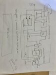
My name is Alex and I'm currently working on a datapath design. The instructions are: Design a system that sum the values stored in a memory from a specific address. The sum system includes the design of and finite state machine (FSM) and a datapath. A test bench is provided to validate your system.

I have already search and done a design but I'm not sure if I'm in the correct way.

My design is the following:
datapath_design.jpg

I understand the coding, so I don't have problem with it.

Thanks!!

This pseucode is the reference of the project

Code:
int sumcalc(int startaddr, int numxfer) {
int sum = 0;
For(i=0; i<numxfer; i++) {
	sum = sum + mem[startaddr+i];
}
return sum;
}


My question is: the code above represent the counter itself? and what is doing with mem[startaddr+i];?
 

i is the counter, the line for sum represents the accumulation of all the data in mem starting from startaddr through startaddr+numxfer-1
 
Therefore, I don't need basically to write it in the Verilog. It is juts an abstract idea for understanding the counter and the sum itself? In other words, the pseucode represent the whole looping of the design.
 

Therefore, I don't need basically to write it in the Verilog. It is juts an abstract idea for understanding the counter and the sum itself? In other words, the pseucode represent the whole looping of the design.

?

I'm assuming that you got the pseudo code as part of your assignment and you are supposed to write Verilog to do what the pseudo code does, i.e. the pseudo code is only to let you know what the algorithm you are designing in Verilog is supposed to do.

The pseudo code is a software-like description of the alghorithm, which is add up numxfer words from a RAM starting at startaddr. Your block diagram sort of looks like it might do the job though there seems to be some missing stuff (from the FSM) not shown.

- - - Updated - - -

I didn't look at it too carefully as I had to tilt my head ;-)
 
Alright!!! That was my problem. Started to look a lot of references and I saw Verilog examples that were using "reg mem[0:255]" and I supposed that I needed to do the same with my code. However, you have already clarified to me the idea of pseucode. Yes, the FSM I'm working on it, but I wanted to be sure that I wasn't missing any other component in the design.

Thanks for your time you helped me a lot!! :) btw, I took the picture from the wrong angle, next time I'll take the picture in landscape mode.
 

Status
Not open for further replies.

Part and Inventory Search

Welcome to EDABoard.com

Sponsor

Back
Top