Continue to Site

Welcome to EDAboard.com

Welcome to our site! EDAboard.com is an international Electronics Discussion Forum focused on EDA software, circuits, schematics, books, theory, papers, asic, pld, 8051, DSP, Network, RF, Analog Design, PCB, Service Manuals... and a whole lot more! To participate you need to register. Registration is free. Click here to register now.

Zero threshold MOSFETs

Status
Not open for further replies.

bio_man

Full Member level 2
Joined
Mar 30, 2010
Messages
144
Helped
2
Reputation
4
Reaction score
4
Trophy points
1,298
Activity points
2,698
Hello All,

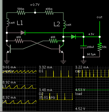
I have a circuit that I want it to startup from a very Low voltage source ( 0.25v). I was able to boost this voltage to a 1v using cross-couples-charge-pump but the problem is that my the nMOS switches I am using needs at least 3V to work efficiently.

I came across a concept of zero-threshold voltage MOSFETs. I want to see if any of you have used these mosfets and how can I layout them ? because the usual MOSFETs will definitely has a Vth of few tens of millivolts.

Also, any tips how can I get the 3V out of my 0.25v source?

Thanks
 

Zero threshold voltage MOSFET are called native transistors. They require special masks. You need to check your process.

Native transistors have larger lengths typically 2x compared to standard threshold voltage transistors.
 
thanks deba_fire. So I guess: the increase in the cost is a reason that makes them undesirable.

Is there any way to compensate for the Vth in normal transistors and makes almost zero effectively? using circuits, nothing to do with the Fabrication process
 

Speaking of cross-coupling, I too used it with transistors and inductors to build a counterpart of the classic astable multivibrator (which is capacitor-based). Then I morphed my oscillator into a twin interleaved boost converter. I tested it in hardware with a battery supply of 1.2V. It works, with light loads.

I have a hunch this won't turn out to be my million dollar idea, so I'm posting it for free at this forum. The concept might be adapted to your cross-coupled charge pump with 0.25V supply.

8931108300_1478117728.png


Some amount of asymmetry is required, so that oscillations start to get going on powerup.
 
Thanks BradtheRad for sharing, it is really appreciated.

for my case, I want to use caps and transistors only ( ultimate goal is to fabricate). I guess you are using inductors to give oscillation and then providing your load with boosted signal after couple of cycles.
I am using also on-chip ring oscillators that provides me with the clocks.

anyway, this is very circuit to have it in mind for some other applications I am working on. thanks man, btw, just curious: what software you are using for the simulation?
 

Caps and transistors only, pretty much limit you to the dc input voltage.
At least with inductors, you get the turn off voltage kick which can be used in many ways to great advantage.
 
One big problem with "zero-VT" MOSFETs is that they are
probably the most poorly controlled of any, in a given PDK.
They suffer the most influence from uncontrolled factors,
being the lightest-doped.

Another practical matter is, if you like to say that VT is
roughly where a one-square device runs 1uA IDsat, then
you have 1uA leakage through it with Vgs=0 - give or
take at least a decade, due to problem #1. If you are
trying to do a nanopower energy harvester (like RFID)
with micropower waste terms, go directly to FAIL, do not
pass Go, do not collect $200.

Zero-VT devices' light (or nil) channel doping fails to push
field back against the LDD effectively, so they break down
lower and leak more than the same-L VT-implanted FET.
They have worse lambda as well for the same reason.

The only reason you find them in PDKs is that you can
"run them hotter" for the same available gate drive, in
RF applications. 50-ohm guys don't care about microamps
of DC leakage (or DC attributes much, at all). But I don't
think this is your case.

And in my little, long-past RFID dabbling and later charge
pump designs, I found the best answer, for a compromise
between forward inefficiency and leak-back inefficiency,
was the "mid-VT" devices I had available, at 200-350mV
VT (between the "0" (that is, -150 - +150mV) and "regular"
(600-700mV) devices, which would lose everything they
gained, and gain nothing at low amplitudes respectively.

Q-boosting with a resonant tank is something you might
be able to take advantage of. But nonetheless, you need
the best balance of forward and slosh-back terms and I
have not seen the zero-VT FET be that.

Fewer technologies have the mid-VT device, or have it
in your sweet spot. But they're worth seeking out.
 
I guess you are using inductors to give oscillation and then providing your load with boosted signal after couple of cycles.

Yes, that's the idea. No need for a separate oscillator or control IC.

A similar thing can be done with the common astable multivibrator (capacitor based). The capacitors provide charge-pump action. I got a small voltage boost, using an arrangement with PNP transistors. The diodes rob a lot of the boost, however.

btw, just curious: what software you are using for the simulation?

Falstad's animated interactive simulator. Free to download and use at:

www.falstad.com/circuit
 
Status
Not open for further replies.

Part and Inventory Search

Welcome to EDABoard.com

Sponsor

Back
Top