Continue to Site

Welcome to EDAboard.com

Welcome to our site! EDAboard.com is an international Electronics Discussion Forum focused on EDA software, circuits, schematics, books, theory, papers, asic, pld, 8051, DSP, Network, RF, Analog Design, PCB, Service Manuals... and a whole lot more! To participate you need to register. Registration is free. Click here to register now.

Minimize the noise on the board

Status
Not open for further replies.

zhangz64

Junior Member level 3
Joined
May 1, 2013
Messages
25
Helped
0
Reputation
0
Reaction score
0
Trophy points
1,281
Activity points
1,632
Hi Everyone,

I am currently struggling to determine the power supply for my board, and would really appreciate some inputs.

the Board i am designing requires a High level of precision and consist of the following sub circuits.
1) High precision Bias Voltage from DAC
2) High precision Bias Current
3) low noise Adjustable power supply.

Therefore, Minimizing noise is really important for those circuits. So Here is what i am proposing.

The board requires approximately 700mA @3.3V maximum.
Since It will not alway operate at maximum, I can power the board with a single host USB for most of the time.( I think usb 2.0 can supply for up to 500mA at 5V)

if more current is required , i will just connect another usb from a wall charger.(diode connection with the usb host).

The problem with those USB supply is that they are somewhat noisy. I do not want those noise to roam on my board, So i put a immediate LDO next to the USB input port to step it down to 4.5Vs and give me a nice clean power supply.

Here are my questions:
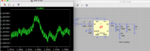
1) Should i use 5V to get 4.5V from master LDO and then use separate LDOs to get 3.3V for each sub circuit(picture 1) ? or does it make a difference to have 5V directly down to 3.3Vs shared for all the sub circuit(picture 2).

2)DO i really need an additional USB supply from wall charger? or A single host usb is enough ? Does my calculation make sense?
( 5V * 500mA / 3.3V = 750mA, and some losses of course from LDO).

3) What other things i should be considering to minimize the noise? (etc,separate digital supply from analog supply ?, layout consideration)

Thanks a lot for the help,
Eddy
Screen Shot 2016-10-25 at 11.00.24 PM.png
Screen Shot 2016-10-25 at 11.00.18 PM.png
 

Consider "noise" a vague term. You should better analyze interference level versus frequency and specify your clean power supply requirements.

Different LDO have different degree of ripple rejection. Ripple rejection at the typical SMPS pwm frequencies is not generally good and mainly achieved by output capacitors. Respectively a good LC filter can give better "noise" rejection in the frequency range > 100 kHz than an additional LDO.

You should also consider that common mode interferences injected by the power supply can be serious problem if your board has any external signal connections (not shown in the block diagram). They require common mode filters.
 
Hi,

First we need values.
requires a High level of precision an
You need to tell us more. What signal (source ... to target) needs to be within what levels.(really values in mV or uV)
Give us the highest noise level you can live with, and give the values you wish to achieve.
(It makes no sense to talk about mV supply noise in a 10 bit /3V precision system.)

Avoiding noise is better than reducing noise:
* use a really proper GND plane, maybe with cuts to divide noisy areas from low noise areas
* if possible: use one clock source and create all necessary clocks from this clock
* synchronize switching regulators to this clock
* avoid multiple (power) inputs

1) expect only 4.5V minimum input voltage from the USB. If you add two with diodes, then the diode voltage drop may down to 4.0V only. I'd go for a single active stage solution: passive filters for the input frequency folofwed by a voltage regulator. I tend to use only one 3V3 regulator for all analog circuitry. But it depends on the circuit.

2) I'm sorry, your power calculation is wrong: As described above you can only calculate with 4.5V or 4.0V input voltage. Current 500mA.
LDOs don't increase the current. The max output current is 500mA.

3) If you really decide to use a second (USB style) power supply, then my recommendation:
* use all the necessary power from only one port
* use common mode filters at the power input. Avoid/break HF loops via the external cabling

Use RC filters in the signal lines.

Check if this is possible: only one power input. Without diode, switch mode regulator to get 3V3 (expect max 650mA). Then use (individual passive low pass filters: RC, LC. LC are more critical because their resonant frequency)

(Modern (synced) switching regulators aren't that bad. For sure they need careful device placement and PCB routing. And -only maybe - passive post filtering. I use this configuration in a 3V3, 16bit ADC system with 1 (maybe 2) LSB precision with 3kHz signal bandwidth.)

Klaus
 
As I have mentioned in other posts, a good board layout is crucial for high performance, which among other things means low noise.

I've personally witnessed that re-routing a board trace a few mm. away, rotating a component 90 degrees, or connecting the ground pin to a different ground location, will reduce noise far more than attempting to cure the problem by brute force.

I can tell you that in particular ANY heavy filter that you include anywhere, will have significant noise on its ground return path.
Therefore............If you happen to connect -let's say- the voltage reference along that same return path, then no amount of extra filtering will remove the noise.

Good board layout, optimized for low noise and/or high frequency, is both a science and a black art.
 
Thanks so much for the detailed reply.

Hi,
You need to tell us more. What signal (source ... to target) needs to be within what levels.(really values in mV or uV)
Klaus

The board has 16 bit DAC with -/+ 1 LSB precision. Also i am using this DAC to generate bias current with V/C convertor. ( 10mV = 10uA, if I want to get 10uA accurately say 5% error, I think i will need to have noise less than 500uV)


Hi,
Check if this is possible: only one power input. Without diode, switch mode regulator to get 3V3 (expect max 650mA). Then use (individual passive low pass filters: RC, LC. LC are more critical because their resonant frequency)
Klaus

Yeah definitely, This is what i was thinking! Ideally i want to have 1 USB as supply and use a buck to get 3.3V
Again, My only concern is the noise, i tried LTC3561A from linear technology and simulated its noise performance.
As you can see, The high frequency ripple is well suppressed with my large output cap. however i do noticed a high low frequency ripple (around 1mV). i suspected that this is from the inductor ripple current, however when i increase the inductance, The noise still present.
Maybe i should use a special LC or RC filter like you suggested?
If you don't mind , could you share what Switch regulators did you end up using?

Another idea i have is that use the BUCK to give me 3.4V and use a LDO to drop to 3.3V.

I found a LDO from AD (ADM7171) that has a dropout voltage of 47mV@500m/3V. I lose some efficiency ,but get a very stable output for all my analog circuits.

I tend to use only one 3V3 regulator for all analog circuitry. But it depends on the circuit.
I plan do that as well, I want to use this stable 3.3V for all my analog circuit.

Thanks a lot,
Eddy
 

Attachments

  • Screen Shot 2016-10-27 at 1.38.34 AM.png
    Screen Shot 2016-10-27 at 1.38.34 AM.png
    465.6 KB · Views: 112

I see that the claimed 700 mA @ 3.3 V demands for a switching regulator if the device should be supplied by USB 2.0. But as KlausST already mentioned, the calculation is unrealistic because it neither reflects the VBUS voltage range nor voltage converter losses.

Demanding minimal noise while trying to operate at the power supply capacity limit doesn't fit well and must be expected to fail. It's no professional design.

You'll may want to rely on optimistic assumptions (no large VBUS variation, short USB cable, some margin in VBUS current limiting). Better you find a way to reduce the 700 mA requirement.

The simulated LTC3561A noise in post #5 spans less than 1 mV and would be no problem with quite a bit of analog supply filtering. But it's just a simulation and if you put the LTC3561A reference design on your board without much circuit design knowledge, you'll easily get the hundredfold noise level.

Using switched mode regulators embedded into a precision signal board is a design challenge. Besides filtering input and output of the switched mode converter, it also involves well considered ground (plane) layout. If you have any chance to reduce the supply current below 500 mA and use pure analog voltage regulation, you are avoiding a lot of trouble.
 
Hi,

I totally agre with FvM.

I want to underline, that 1mV ripple in supply voltage doesn´t mean 1mV ripple in signal voltage.
Unfortunately Opamps and DACs don´t have high attenuation of high frequency power supply ripple (PSRR), on the other hand passive filters RC, LC have very good high frequency attenuation.


The board has 16 bit DAC with -/+ 1 LSB precision. Also i am using this DAC to generate bias current with V/C convertor. ( 10mV = 10uA, if I want to get 10uA accurately say 5% error, I think i will need to have noise less than 500uV)
It seems you talk about noise as if it was DC.

The noise won´t harm DC performance. The noise just can be filtered out.
The problem is when noise frequency is in the range of the desired signal frequency range.
Therefore we need to know your signal frequency bandwidth.

To keep signal noise below 500uV shouldn´t be a problem. (500nV is a challenge ;-) ).

Bias voltage or current sound like very low frequency. So: relax.

Klaus
 

To wrap up what Klaus and FvM mentioned;

Remember that many inductors radiate stray magnetic fields. Those fields can and will induce noise on adjacent board traces. That is the reason you should be careful about its location and/or orientation.

Or use inductors which are built specifically with low stray field cores. I. e. toroids or PQ (pot) cores.
The worst offenders are inductors with rod cores. Since they are also the lowest cost, many unsuspecting users choose them.
 

Status
Not open for further replies.

Similar threads

Part and Inventory Search

Welcome to EDABoard.com

Sponsor

Back
Top