Continue to Site

Welcome to EDAboard.com

Welcome to our site! EDAboard.com is an international Electronics Discussion Forum focused on EDA software, circuits, schematics, books, theory, papers, asic, pld, 8051, DSP, Network, RF, Analog Design, PCB, Service Manuals... and a whole lot more! To participate you need to register. Registration is free. Click here to register now.

[SOLVED] Testing of DAC outputs

Status
Not open for further replies.

RAJPUT VIDISHA

Member level 1
Joined
Jul 14, 2015
Messages
37
Helped
0
Reputation
0
Reaction score
1
Trophy points
6
Activity points
344
Hi,

i'm working with PIC16F1777 device & I want to test DAC outputs (RC0, RE1, RA5, RA2 to 1.8, 2.2, 2.5, 3.0V respectively)
I don't have any idea about DAC & how to do approach also..
Please can anyone guide me..

Thanks
Vidisha
 

Hi,

Just set the DAC to the desired value according datasheet, then use a multimeter to test if the output meets your setup.

I don´t understand where you see a problem.

Redaing the datasheet is urgent.
If you have further questions it is best, if you refer to the chapter in the datasheet.

Klaus
 
  • Like
Reactions: Okada

    Okada

    Points: 2
    Helpful Answer Positive Rating
Thanks for replying but still im not getting the point..

is there any example to refer..i already searched in net but couldnot find proper one..
 

5 Bit DAC

DAC1CON0 = 0b10110000
DAC3CON0 = 0b10110000
DAC4CON0 = 0b10110000
DAC7CON0 = 0b10110000
DAC8CON0 = 0b10110000


5V = 32


1.8 = 12 = DAC1REF
2.2 = 14 = DAC3REF
2.5 = 16 = DAC4REF
3.0 = 19 = DAC7REF

10-Bit DAC

DAC1
DAC2
DAC5
DAC6

DAC1CON0 = 0b10110000
DAC2CON0 = 0b10110000
DAC5CON0 = 0b10110000
DAC6CON0 = 0b10110000

5V = 1024

1.8 = 368
2.2 = 450
2.5 = 511
3.0 = 614

DAC1REFL = 0x70
DAC1REFH = 0x01

DAC2REFL = 0xC2
DAC2REFH = 0x01

DAC5REFL = 0xFF
DAC5REFH = 0x01

DAC6REFL = 0x66
DAC6REFH = 0x02
 

Hi,

i already searched in net

I´m sure it´s all given in the datasheet. No need to search the whole internet.
Datasheet tells you all. The manufacturers don´t hide informations, instead they give you all informations so you are motivated to use their parts.

Klaus
 
  • Like
Reactions: Okada

    Okada

    Points: 2
    Helpful Answer Positive Rating
Here is the code which I made for your MPLAB X XC8 Compiler. There is one bug in XC8. INLVLE register usage is giving error even though the device has that register.


Code C - [expand]
1
2
3
4
5
6
7
8
9
10
11
12
13
14
15
16
17
18
19
20
21
22
23
24
25
26
27
28
29
30
31
32
33
34
35
36
37
38
39
40
41
42
43
44
45
46
47
48
49
50
51
52
53
54
55
56
57
58
59
60
61
62
63
64
65
66
67
68
69
70
71
72
73
74
75
76
77
78
79
80
81
82
83
84
85
86
87
88
89
90
91
92
93
94
95
96
97
98
99
100
101
102
103
104
105
106
107
108
109
110
111
112
113
114
115
116
117
118
119
120
/*
 * File:   Using DACs of PIC16F1777
 * Author: Okada
 * 
 * Created on October 19, 2016, 5:08 PM
 */
 
#define _XTAL_FREQ 32000000
 
#include <xc.h>
 
// CONFIG1
#pragma config FOSC = INTOSC    // Oscillator Selection Bits (INTOSC oscillator: I/O function on CLKIN pin)
#pragma config WDTE = ON        // Watchdog Timer Enable (WDT enabled)
#pragma config PWRTE = ON       // Power-up Timer Enable (PWRT disabled)
#pragma config MCLRE = ON       // MCLR Pin Function Select (MCLR/VPP pin function is MCLR)
#pragma config CP = ON          // Flash Program Memory Code Protection (Program memory code protection is disabled)
#pragma config BOREN = ON       // Brown-out Reset Enable (Brown-out Reset enabled)
#pragma config CLKOUTEN = OFF   // Clock Out Enable (CLKOUT function is disabled. I/O or oscillator function on the CLKOUT pin)
#pragma config IESO = ON        // Internal/External Switchover Mode (Internal/External Switchover Mode is enabled)
#pragma config FCMEN = ON       // Fail-Safe Clock Monitor Enable (Fail-Safe Clock Monitor is enabled)
 
// CONFIG2
#pragma config WRT = OFF        // Flash Memory Self-Write Protection (Write protection off)
#pragma config PPS1WAY = ON     // Peripheral Pin Select one-way control (The PPSLOCK bit cannot be cleared once it is set by software)
#pragma config ZCD = OFF        // Zero-cross detect disable (Zero-cross detect circuit is disabled at POR)
#pragma config PLLEN = ON       // Phase Lock Loop enable (4x PLL is always enabled)
#pragma config STVREN = ON      // Stack Overflow/Underflow Reset Enable (Stack Overflow or Underflow will cause a Reset)
#pragma config BORV = LO        // Brown-out Reset Voltage Selection (Brown-out Reset Voltage (Vbor), low trip point selected.)
#pragma config LPBOR = ON       // Low-Power Brown Out Reset (Low-Power BOR is disabled)
#pragma config LVP = OFF        // Low-Voltage Programming Enable (Low-voltage programming enabled)
 
#define LED LATDbits.LATD0
 
void main(void) {
    
    OSCCON = 0b01111010;
        
    CM1CON0 = 0x00;
    CM2CON0 = 0x00;
    CM3CON0 = 0x00;
    CM4CON0 = 0x00;
    CM5CON0 = 0x00;
    
    ANSELA = 0x00;
    ANSELB = 0x00;
    ANSELC = 0x00;
    ANSELD = 0x00;
    ANSELE = 0x00;
    
    ODCONA = 0x00;
    ODCONB = 0x00;
    ODCONC = 0x00;
    ODCOND = 0x00;
    ODCONE = 0x00;
    
    INLVLA = 0x00;
    INLVLB = 0x00;
    INLVLC = 0x00;
    INLVLD = 0x00;
    //INLVLE = 0x00;
    
    SLRCONA = 0x00;
    SLRCONB = 0x00;
    SLRCONC = 0x00;
    SLRCOND = 0x00;
    SLRCONE = 0x00;
    
    WPUA = 0x00;
    WPUB = 0x00;
    WPUC = 0x00;
    WPUD = 0x00;
    WPUE = 0x00;
        
    TRISA = 0xC0;
    TRISB = 0x00;
    TRISC = 0x00;
    TRISD = 0x00;
    TRISE = 0x00;
    
    PORTA = 0x00;
    PORTB = 0x00;
    PORTC = 0x00;
    PORTD = 0x00;
    PORTE = 0x00;
    
    LATA = 0x00;
    LATB = 0x00;
    LATC = 0x00;
    LATD = 0x00;
    LATE = 0x00;
    
    OPA1CON = 0x00;
    OPA2CON = 0x00;
    
    DAC1CON0 = 0b10100000;
    DAC2CON0 = 0b10100000;
    DAC5CON0 = 0b10100000;
    DAC6CON0 = 0b10100000;
    
    DAC1REFL = 0xFF;
    DAC1REFH = 0x01;
    
    DAC2REFL = 0x66;
    DAC2REFH = 0x02;
    
    DAC5REFL = 0x70;
    DAC5REFH = 0x01;
    
    DAC6REFL = 0xC2;
    DAC6REFH = 0x01;    
    
    DACLD = 0x00;
    
    while(1){
        
        LED = ~LED;
        __delay_ms(500);
    }
}


Attachments

  • Using DACs of PIC16F1777.X.rar
    161.9 KB · Views: 50
Last edited:

For Pins used for Dac Outputs you have to set ANSELx bits to 1.
 

I made this project and tested it in hardware (EasyPIC v7) but didn't get correct voltages. Code is correct, maybe Compiler is generating wrong .hex file.

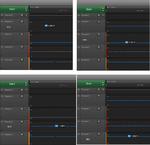
Voltages measured using Saleae Logic.

If anybody has XC8 Compiler then please make a copy of my .hex file and clean and compile the project in free mode and compare the generated .hex file with my .hex file and tell me if there are any differences. I want to make sure compiler is generating correct .hex file. I am using latest version of MPLAB X and XC8 Compiler.
 

Attachments

  • Using 10 Bit DACs of PIC16F1777.X.rar
    918.7 KB · Views: 47
  • DAC Outputs.png
    DAC Outputs.png
    82.4 KB · Views: 93
Last edited:

Hi,

1024 = 5V.

Did you measure those 5V at VREF pin?
For me it seems your Vref is about 4.25V only.

If the 5V have any error in % for sure the same error is at the outputs.

Klaus
 
  • Like
Reactions: Okada

    Okada

    Points: 2
    Helpful Answer Positive Rating
Hi KlausST

I have set VDD as Vref+ and VSS as Vref-. I am using only 10 bit DACs on RA2, RA5, RC0, RE1. Only DACxOUT1 outputs are used. I am using PDIP version of PIC16F1777 E/P. VDD is 3.3V and hence vref+ for DACs are 3.3V. The values generated and assigned to DACxREFH and DACxREFL registers by Microchip Code Configurator (MCC) are correct. I have checked them individually. I have also checked ANSELx register settings. Everything seems to be correct. On EasyPIC v7 development board I have set VDD as 3.3V. All connections are correct but not getting correct voltages.

I have to get 3.0, 2.5, 1.8 and 2.2V on RA2, RA5, RC0 and RE1 respectively.

I am blinking LED at RD0 once every 500 ms and it is working fine. Only problem is with DAC outputs.

I have 2x new PIC16F1777 and I used both for testing but same result and so PICs can't be defective.

I have doubt that Compiler is generating incorrect .hex file.

For DACxREFH and DACxREFL I am using right justified data.
 
Last edited:

Hi,

independent of your setup and oyur estimations....

* did you MEASURE the voltage at VDD? Is it precise 3.3V (during DAC output voltage measurement)?
* Is your DAC output loaded with any current (resistor...)
* does your PIC getting warm/hot?

Debug: Set any unconncted port output to HIGH and measure it´s voltage.

Klaus
 

* did you MEASURE the voltage at VDD? Is it precise 3.3V (during DAC output voltage measurement)?

Yes, It is 3.2998V

* Is your DAC output loaded with any current (resistor...)
No, There are no load resistors. I have also disabled Weak Pullup resistors. I am just measuring the voltage at DAC output pins w.r.t GND.

* does your PIC getting warm/hot?
No, PIC doesn't get hot. I tested for 5 minutes. I have LED blinking at 500 ms rate and I see it working and the voltage at LED pin toggles between 3.288V and 0V.

I measured the data for 3 seconds using Saleae Logic Oscilloscope.

All settings (jumper settings) on the EasyPIC v7 board are correct. Only 10 bit DAC output voltages are not correct. I tested 5 bit DAC outputs and they give correct voltages.

If anybody has XC8 Compiler please compile my project and post the .hex file. I will burn it and test again.

- - - Updated - - -

Should I use a Unity Gain Amplifier for each DAC output ?
 

Hi,

Should I use a Unity Gain Amplifier for each DAC output ?

you should not draw significant current form the DAC output.

If you need current: then yes, you need an amplifier.

****
I just reviewed the schematics of EASY_PIC V7.
Just as fro DAC2 output: (do the same with the other DAC outputs)
* be sure SW6.1 is OPEN
* be sure CN14.RB7 is not connected
* be sure CN9.RB7 is not connected
* be sure CN19.RB7 is not connected
* be sure CN24.RB7 is not connected
* be sure SW2.6 is OPEN
* be sure JP9.RB7 is OPEN (BRD-PGD)
* be sure SW3.2 is OPEN

If you changed anything: do a new voltage test at DAC2 output.


Klaus
 
  • Like
Reactions: Okada

    Okada

    Points: 2
    Helpful Answer Positive Rating
@KlausST.

Ok. I will try.

Here I am attaching modified project. I was not able to configure OPA1 as unity gain amplifier whose Inverting input is tied to output of OPA1 and Non-Inverting input is internally tied to DAC1OUT1. Please tell me how to configure it.

Will these settings give 3.3V at OPA1OUT ?

Code:
OPA1CON = 0b10010000
OPA1ORS = 0x00
OPA1NCHS = 0x0F
OPA1PCHS = 0b00000010	(DAC1_out as input to OPA1 Non-Inverting input)

DAC1CON0 = 0b10000000
DAC1REFH = 0x03
DAC1REFL = 0xFF
DACLDbits.DAC1LD = 1

DAC Vref+ = VDD = 3.3V
DAC Vref- = VSS = 0V

10 Bit DAC (Internal DAC and Internal Op Amp)

Will this settings give me 3.3V at OPA1OUT ?

I have not shown ANSELx settings for OPA1OUT pin. It will be set to analog output. If these settings are not correct then please tell me what changes I have to do to use OPA1 as Unity Buffer with internally connecting DAC1OUT to OPA1 non-inverting input to get 3.3V at OPA1OUT.
 

Attachments

  • Using 10 Bit DACs of PIC16F1777 RevB.X.rar
    918.8 KB · Views: 41
Last edited:

I created a new project and used Microchip Code Configurator to generate the code. I used only DAC1 and OPA1. I connected DAC1 out internally to OPA1 non inverting input and configured OPA1 as unity gain amplifier. OPA1OUT pin RA1 was configured as analog output pin. DAC Vref+ was set to VDD = 3.3V and Vref- was set to VSS = 0V. DAC was configured to ouput 3V and OPA1 to output this 3V but I got this signal on OPA1OUT (RA1). See image.
 

Attachments

  • Using Op Amps of PIC16F1777.X.rar
    663.8 KB · Views: 48
  • dac to opamp.png
    dac to opamp.png
    36.7 KB · Views: 80

Status
Not open for further replies.

Similar threads

Part and Inventory Search

Welcome to EDABoard.com

Sponsor

Back
Top