Continue to Site

Welcome to EDAboard.com

Welcome to our site! EDAboard.com is an international Electronics Discussion Forum focused on EDA software, circuits, schematics, books, theory, papers, asic, pld, 8051, DSP, Network, RF, Analog Design, PCB, Service Manuals... and a whole lot more! To participate you need to register. Registration is free. Click here to register now.

(Mixer design) IFp and IFn have same phase

Status
Not open for further replies.

ktx2222

Member level 5
Joined
Jan 8, 2014
Messages
81
Helped
2
Reputation
4
Reaction score
2
Trophy points
8
Activity points
613
Hi all,

I have design a double balanced Gilbert cell mixer.

In ADS, the output IFp and IFn are 180 deg out of phase.

Then I simulate in Cadence, the problem is that the IFp and IFn signals are in phase. I think that is the reason why the conversion gain is smaller than 0 dB.

I have spent couple of days but I cannot figure out the reason. Please help! Thank you so much.
 

Some common mode signal can be expected, but not much. We can just guess that you made something seriously wrong, e.g. wrong bias point.

Can't say more without substantial information.
 

Thank you for your replies,

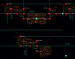
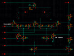
My schematic and testbench:

schematic.jpg

testbench.jpg
 

Next point is to show input signals, bias voltages and currents, observed node signals.
 

Operating bias point:
bias.jpg

LO input signal (-5 dBm)
LO.jpg

RF input signal (-50 dBm)
RF.jpg

IF output signal
IF.jpg
 

Hopefully the top transistors have sufficient Vds margin, too.

We see a lot of crosstalk, e.g. at the RF input terminals. The output signal is probably just the sum of parasitic effects.
Is the design suited for 5 GHz by layout parameters?

Are you intending frequency doubling or IF mixing? In the latter case, what's the expected output frequency? Can it pass the output transformer?

Did you operate the mixer with moderate RF and LO frequencies to verify it's function?
 

RFp and RFn interacts each other on the bias node.Put a large capacitor on bias net
 

Hi FvM, thank for your reply

Hopefully the top transistors have sufficient Vds margin, too.
I tried to design low power mixer, so the top transistor (Switching transistor) was biased at: Vd = 1 V, Vs = 0.654 V, Vg(max) = 1.25 V (because of LO swing), Vth = 0.477 V

We see a lot of crosstalk, e.g. at the RF input terminals. The output signal is probably just the sum of parasitic effects. Is the design suited for 5 GHz by layout parameters?
Are you intending frequency doubling or IF mixing? In the latter case, what's the expected output frequency? Can it pass the output transformer?
fLO = 4.9 GHz, fRF = 2.5 GHz, fIF = 2.4 GHz. Would you please tell me how to overcome the crosstalk problem? I assume that I have ideal balun and I want to check the function of mixer first.

Did you operate the mixer with moderate RF and LO frequencies to verify it's function?
I will follow this instruction.

- - - Updated - - -

RFp and RFn interacts each other on the bias node.Put a large capacitor on bias net

In fact, I changed the RF port to DC source type. I only simulate the transient with LO signal. The problem still happens.
 

fLO = 4.9 GHz, fRF = 2.5 GHz, fIF = 2.4 GHz.
Doesn't fit your post. In your waveforms, fLO and fRF are apparently both near 5 GHz.

In fact, I changed the RF port to DC source type. I only simulate the transient with LO signal. The problem still happens.
Doesn't make sense. Of course, DC level must be applied to the gates directly, without coupling capacitors. Trace the individual drain currents to understand how the output is generated.
 

Doesn't fit your post. In your waveforms, fLO and fRF are apparently both near 5 GHz.

Doesn't make sense. Of course, DC level must be applied to the gates directly, without coupling capacitors. Trace the individual drain currents to understand how the output is generated.

I am sorry, I made you confuse.

1. I separately bias the mixer with VDC sources. I put 10nF caps at inputs/outputs to block DC current.

2. Sometime I removed the RF signal (by change the source type of RF port to dc) to see the effect of LO signal.

The following picture I ran with fLO =4.9 GHz, pLO = -5 dBm, fRF = 2.5 GHz, pRF = -50 dBm. I expect the output is fIF = 2.4 GHz and the conversion gain is 10 dB (from ADS simulation)

LO input
1.jpg
RF input
2.jpg
IF output
3.jpg
 

your positive and negative RF signals DC changes during time
You see feedthrough of 2nd LO harmonic.

I put 10nF caps at inputs/outputs to block DC current.
Might have no effect if the balun output has high common impedance (transformer winding with floating center tap).
 

clock feedthrough have this much effect in the input ?

In other mixers like passive RL mixer, it effects input with 2WLo but here we have one Cgs and Cgd, it should not effect this much :/

2Wlo mixes with Wlo and if it is zero IF structure it will be filtered out.

- - - Updated - - -

pleas take a screen shot from all of ur circuit not a part.
 

Might have no effect if the balun output has high common impedance (transformer winding with floating center tap).

Anw, the 10nF caps do not explain why IFP and IFN have same phase.

- - - Updated - - -

clock feedthrough have this much effect in the input ?

In other mixers like passive RL mixer, it effects input with 2WLo but here we have one Cgs and Cgd, it should not effect this much :/

2Wlo mixes with Wlo and if it is zero IF structure it will be filtered out.

- - - Updated - - -

pleas take a screen shot from all of ur circuit not a part.

You can see the full schematic in reply #4 in this thread. If I misunderstand what you mean, please explain
 

Have you ever checked there is no 2nd frequency in RF port ?? There is a beating between two frequencies ( looks like it )
 

Anw, the 10nF caps do not explain why IFP and IFN have same phase.
Not particularly the caps. But a RF port common mode signal will be translated to an output common mode signal, just think. So my latest question was if your balun might be unsuitable by a exposing a high common output impedance and thus promoting feedthrough of the 2nd LO harmonic generated by MN0-MN3 non-linearity.

To rate the measured voltage levels, it would be interesting to know the output "transformer" self- and mutual inductance.
 

In the design of mixer u should become sure that:

1) RF transistor works in sat.

2) In half cycle one of LO transistors is off and the other one is on and other half wise versa.

3) While two LO transistors are on (middle of 2 cycles) they should be forced to work in saturation until the moment when one of them turns on and other one turns off.


Anw, the 10nF caps do not explain why IFP and IFN have same phase.

- - - Updated - - -


You can see the full schematic in reply #4 in this thread. If I misunderstand what you mean, please explain

Do you understand clock feedthrough ?
 

Status
Not open for further replies.

Part and Inventory Search

Welcome to EDABoard.com

Sponsor

Back
Top