Continue to Site

Welcome to EDAboard.com

Welcome to our site! EDAboard.com is an international Electronics Discussion Forum focused on EDA software, circuits, schematics, books, theory, papers, asic, pld, 8051, DSP, Network, RF, Analog Design, PCB, Service Manuals... and a whole lot more! To participate you need to register. Registration is free. Click here to register now.

[SOLVED] How to design an efficient high power bilateral switch for this special purpose?

Status
Not open for further replies.

Alper özel

Member level 1
Joined
Feb 28, 2015
Messages
40
Helped
0
Reputation
0
Reaction score
0
Trophy points
6
Location
Turkey / Scotland
Activity points
487
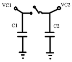
I need to design a system that equalizes the two capacitors on each side. There are two big capacitors in the system and they will be charging and discharging by out of the system. They might reach to 105V and down to GND at any time. We won't know that, I am only responsible for equalizing the capacitor voltages by an interrupt input.
EDA1.png
For simplicity I draw the figure above. VC1 and VC2 may have the voltage level of 0 to 105 sererately at any time!


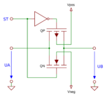
The thing is, I can not consume much power, I have to be efficient. So selenoid and other inefficient switching solutions don't work here. I would use transmission gates(like in the figure below) to do it if capacitor potentials were not allowed to exceed 20V (Due to VGSVGS limitations) but it is not a fit for this system either. So, is there any energy efficient method to allow bilateral current transmission? (In OPEN State there will be no current flow, in CLOSED State Current will flow from high potential to the lower potential)
EDA-TG.png

Thanks in advance.
 

How much time will you be given, to do the equalization
and to what residual accuracy / extent? Do you have to
get it all done in one cycle, and to what residue?

If this is a slow process then something like a photoMOS
type AC relay could do (if you can find one). A low power
reed relay (with proper current limiting and snubbing) is
not to be dismissed out of hand, if energized "just long
enough" it may not be as inefficient as you think and
much more forgiving of things like polarity reversal and
short term voltage overstress. Just what is "much" power
that you cannot consume? Numbers are the beginning of
rational choices.
 
You say "high power" without mentioning required switch current, charge amount or charge times. Up to now it's only high voltage (e.g. 105 V). I would use a 200V DC solid state relay with current limiting resistor.
 
I would use two high power mosfets in inverse series.
That is, both sources tied directly together, both gates tied directly together, and the two drains are the input and output of your switch.

This works both ways for either ac or full bi directional dc switching.
Gate power will be minimal, but a floating voltage source will be required to turn on both mosfet gates together.

Something must be provided to limit the peak current to prevent disaster when switching high differential voltage together.
That could (?) be just Rdson, if the voltages are quite low. A suitable inductor would be a much better solution, but the circuit may then ring for many cycles before it finally settles down. But its the safest and most efficient method if you have the allowed switching time to do it.

Another possibility might be very slow turn on, allowing the mosfets to dissipate substantial power. But that may be far from ideal.

The best final solution depends on the constraints you have, and what this is all supposed to do.

If isolated gate drive power is also a real limitation, the most energy efficient might be a pulse transformer and rectifier to drive the gates.
 
How much time will you be given, to do the equalization
and to what residual accuracy / extent? Do you have to
get it all done in one cycle, and to what residue?

As soon as possible. And yes, I have to do it in one cycle. If you meant the tolerance by 'residue' I don't think I have a big tolerance. The capacitors must be as equal as possible in voltage level when the process is done.
Just what is "much" power
that you cannot consume?

I will use logic and analog structures to control this logic. Logic supply is 5V and System voltage is 105V. I think 0.5 Watt and above must be considered High power for the switching operation in this application.

You say "high power" without mentioning required switch current, charge amount or charge times.

Switch Current may change but I can say that will be up to 10 A and mostly around 6-7 A peak from one capacitor to another.

If isolated gate drive power is also a real limitation, the most energy efficient might be a pulse transformer and rectifier to drive the gates.

I did not limit myself as long as they are efficient but I could not quite understand your suggestion.
 

back to back SCR's (1000A surge rating) a small air cored choke to limit di/dt and some small series resistance to damp out the Q of the L and the C, by far the safest solution...
 

Status
Not open for further replies.

Part and Inventory Search

Welcome to EDABoard.com

Sponsor

Back
Top