CataM
Advanced Member level 4
- Joined
- Dec 23, 2015
- Messages
- 1,275
- Helped
- 314
- Reputation
- 628
- Reaction score
- 312
- Trophy points
- 83
- Location
- Madrid, Spain
- Activity points
- 8,409
Hello everyone,
I was reading in Sedra's book about discrete amplifiers with MOSFETs and at one point he stated this:
In order not to disturb the dc bias current and voltages, the signal to be amplified,
shown as voltage source vsig with an internal resistance Rsig, is connected to the gate through
a large capacitor CC1. Capacitor CC1, known as a coupling capacitor, is required to act as a
perfect short circuit at all signal frequencies of interest while blocking dc
In this special case (schematic below), I do not see its need since the DC bias can not interact with the voltage applied to the gate. Is it because the Vsig could have some sort of DC even though it is an AC voltage source?
Also, later on, he states the following:
Before leaving CC1 (refers to capacitor CC1 in the schematic), we should point out that when the signal source can provide an appropriate dc path to ground, the gate can be connected directly to the signal source and both RG and CC1 can be dispensed with.
I do not understand the reason behind having a dc path to ground in the gate network in this case and how would a signal source provide a dc path to ground.
Could anyone kindly explain ? Thank you !
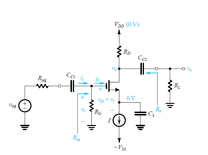