Continue to Site

Welcome to EDAboard.com

Welcome to our site! EDAboard.com is an international Electronics Discussion Forum focused on EDA software, circuits, schematics, books, theory, papers, asic, pld, 8051, DSP, Network, RF, Analog Design, PCB, Service Manuals... and a whole lot more! To participate you need to register. Registration is free. Click here to register now.

Are there EMI problems with this Layout ?

Status
Not open for further replies.

hallo99

Newbie level 6
Joined
Jul 8, 2005
Messages
12
Helped
0
Reputation
0
Reaction score
0
Trophy points
1,281
Activity points
1,389
Hello,

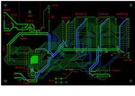
could someone tell me if there is a EMI problem to expect with this 8051 circuit layout ?
It runs at 6MHz clock and the buses should run at 500kHz.

I messed the placing of the decoupling capacitor at the 8051 cpu, i think it should have been above the CPU and connected via a top layer strip to GND under the CPU. At its current position it may form a loop area.

My fear is that this circuit could interfere with my neighbours consumer electronics or DCF clocks for example.


Could you please help me with this ?
 

Attachments

  • 8051 Circuit.jpg
    8051 Circuit.jpg
    151.6 KB · Views: 79

If you want to minimize EMI, flood unused areas with copper ground and stitch the ground with many, many vias. Also, I would increase the widths of some of your traces, especially the really thin ones. It drops the impedance of the lines way down, making them less likely to radiate.

It's hard to evaluate your circuit board layout without a schematic. I don't see the decoupling cap that you mentioned. You might want to put some SMT caps from the 8051 VCC to gnd as close to the device as you can. Same goes for the other digital chips - or any chip, for that matter.

For top/bottom cross-over traces, route them so that they are orthogonal to each other (90°) to minimize coupling.

At your freqs, I really wouldn't worry too much about EMI issues with common sense layout techniques.

Overall, I would say your board is good/very good in layout. Addressing some of my concerns would make it even better.
 

Hi,

My opinion is different.

I don't like copper pours. They can't replace a solid ground plane.
In my eyes for a good EMI/EMC complient design a solid ground plane is a must.

I don't think that the trace width has more than marginal influence on EMI/EMC.

So - sorry for my opinion - i don't think it is a good layout regarding EMC.

Klaus

- - - Updated - - -

Added:

Back in the seventies a layout like this maybe was acceptable.
The frequencies on the board were smaller...maybe 1 MHz, but this 1MHz is not the problem.
The problem are the overtones. And nowadays ICs are faster. Faster in rise time and therefore they generate more overtones.

To send out 1MHz with high power you need an antenna length of 75m (lambda/4). Very unlikely on a PCB.
But the overtones of modern ICs may reach to several 100MHz. And then the antenna length is only a couple of cm.

Sending out is EMI, receiving is EMC.
In the seventies there were no GHz frequencies. But nowadays it is available everywhere: cellular phones, bluetooth, wlan, microwave ovens....
Therefore now your EMC layout needs to take care about those high frequencies.

Klaus
 

I don't like copper pours. They can't replace a solid ground plane.
In my eyes for a good EMI/EMC complient design a solid ground plane is a must.

This is a two sided board. Therefore, there cannot be any solid ground plane. A well stitched together group of copper pours is way better than nothing. I have had many a design that were built without a single, solid ground plane layer, but were built with the multiple pour/stitching method. These designs were all complient with strict, regulatory EMI/EMC standards. Only my microwave designs had a dedicated ground plane (µstrip), but these were also enclosed in metal boxes with no leakage. Also, this will make your ground a much lower impedance, which will greatly reduce issues with the ground being at different potentials across the board.

I don't think that the trace width has more than marginal influence on EMI/EMC.

Marginal influence maybe, but I like the thicker lines where possible. You should treat every line with high frequency data/signal as a transmission line.

So - sorry for my opinion - i don't think it is a good layout regarding EMC.

Don't apologize for your opinion. It's just as valid as anyone else's. I believe that if the OP addresses the grounding, he will have little problem with EMI, especially at a 6MHz clock and 500kHz busses. But only time will tell once he builds and tests the thing.
 

I want to fit this PCB in a box with conducting walls of some kind, but the top side will be open at runtime because there is an I/O board stacked above the CPU board. I think i sandwitch some metal plate between the CPU and I/O board and ground it like the case via a 1MOhm resitor to the ground of the outlet connector. This could also serve as grounding of spikes when touching the I/O board.

I have already the manufactured PCB so i cannot change it, i simply did not know what strenght the EMI of such a circuit could have.


This are all 74HC circuits (the 8051 switching speed is unknown but the port drivers are some special stuff with pullups and so) so i think the expected overall switching speed is in the 10ns range as far as i know.
 

Hi,

I'm sure the design works. It works at home, it works in the laboratory. But is it reliable?

The headline question is only about EMI. I'd say there is a chance it fails the EMI test, even with the low switching frequencies.

But the design is far away to pass an EMC test.
And the EMC test says how reliable it works when there is a cellular phone nearby, or any other HF source.
And EMC is independent of what frequencies you use in your circuit.

I've build electronics equippment for chemical plant (even double sided designs). They need to work 7/24. A single failure may cause to loose a complete production batch, which means several 10000 $.

Klaus
 

Those signals passing underneath the crystal oscillator are a no no too.
 

This 8051 type has some nasty pinout, the two signals under the oscillator should be /RD and /WR but i saw that the oscillator is in a metal case that is connected to its GND pin so it may be not that bad for the trace under it.

The decoupling capacitor at the right side of the CPU is bad placed, i put it there after someone in another forum told me to :)
Maybe it forms a loop and pollutes the whole bus.
 

I have already the manufactured PCB so i cannot change it, i simply did not know what strenght the EMI of such a circuit could have.

You do know that the time to ask for help like this is BEFORE you send your board out for fab. All we can do for you post-fab is make suggestions on getting your second board pass to have better performance in passing the EMI/EMC testing.
 

Why have you routed pin 20 of the memory devices as you have! Moving pin 21 routing down would have saved all those silly vias.
 

Status
Not open for further replies.

Part and Inventory Search

Welcome to EDABoard.com

Sponsor

Back
Top