Continue to Site

Welcome to EDAboard.com

Welcome to our site! EDAboard.com is an international Electronics Discussion Forum focused on EDA software, circuits, schematics, books, theory, papers, asic, pld, 8051, DSP, Network, RF, Analog Design, PCB, Service Manuals... and a whole lot more! To participate you need to register. Registration is free. Click here to register now.

adc spartan 3e interafacing

Status
Not open for further replies.

bitu_tzp

Newbie level 4
Joined
Sep 4, 2016
Messages
5
Helped
0
Reputation
0
Reaction score
0
Trophy points
1
Activity points
125
hello i m student currently working on embedded system design. i have to deal with lots of analog signals, so i require to interface an adc with fpga. for that i ve tried with the onboard adc of spartan 3e. i tried and programmed it many times but the output which adc is showing does not match with the theoretical formula based value. any help regarding my problem will be appreciated. thanks
 

Hi,

You should give us the chance to help. With good informations.
With your given informations
* we don't see what hardware and external circuity you use (maybe there is an issue with your hardware)
* we don't see what you have programmed so far (maybe there is an issue with your program. Setup? Timing?)
* we don't know what you expect (maybe what you expect is wrong)
* we don't see the results of the ADC output (maybe they are correct)

Klaus
 
I received this in a PM, which is a violation of forum rules, but I'm feeling nice about posting it...
I refused to look at the code as it wasn't using syntax/code tags resulting in this poorly formatted mess.

hello sir, i m student currently working on fpga design. i have to deal with lots of analog signals, so i require to interface an adc with fpga. for that i ve tried with the onboard adc of spartan 3e. i tried and programmed it many times but the output which adc is showing does not match with thr theoretical formula based value. Sir, please help me solve my problem. thanks

also i ve used same spi_sck for both adc and amp, its 5MHz

my code is:


Code Verilog - [expand]
1
2
3
4
5
6
7
8
9
10
11
12
13
14
15
16
17
18
19
20
21
22
23
24
25
26
27
28
29
30
31
32
33
34
35
36
37
38
39
40
41
42
43
44
45
46
47
48
49
50
51
52
53
54
55
56
57
58
59
60
61
62
63
64
65
66
67
68
69
70
71
72
73
74
75
76
77
78
79
80
81
82
83
84
85
86
87
88
89
90
91
92
93
94
95
96
97
98
99
100
101
102
103
104
105
106
107
108
109
110
111
112
113
114
115
116
117
118
119
120
121
122
123
124
125
126
127
128
129
130
131
132
133
134
135
136
137
138
139
140
141
142
143
144
145
146
147
148
149
150
151
152
153
154
155
156
157
158
159
160
161
162
163
164
165
166
167
168
169
170
171
172
173
174
175
176
177
178
179
180
181
182
183
184
185
186
187
188
189
190
191
192
193
194
195
196
197
`timescale 1ns / 1ps
//////////////////////////////////////////////////////////////////////////////////
// Company:
// Engineer:
//
// Create Date: 11:40:46 08/30/2016
// Design Name:
// Module Name: adc_sprtn
// Project Name:
// Target Devices:
// Tool versions:
// Description:
//
// Dependencies:
//
// Revision:
// Revision 0.01 - File Created
// Additional Comments:
//
//////////////////////////////////////////////////////////////////////////////////
module adc_sprtn(clk,miso,mosi,amp_cs,spi_sck,amp_shdn,co nv,ssb,ceo,initb,val,val1,state);
input clk,miso;
output mosi,amp_cs,spi_sck,amp_shdn,conv,ssb,ceo,initb;
output [13:0] val,val1;
output [1:0] state;
 
wire w1;
 
clk_div d1(clk,w1);
try2 t1(w1,miso,mosi,amp_cs,spi_sck,amp_shdn,conv,ssb,c eo,initb,val,val1,state);
 
endmodule
 
 
module try2(clk,miso,mosi,amp_cs,spi_sck,amp_shdn,conv,ss b,ceo,initb,val,val1,state);
 
input clk,miso;
output mosi,amp_cs,spi_sck,amp_shdn,conv,ssb,ceo,initb;
output [13:0] val,val1;
output [1:0] state;
reg [7:0] gain=8'b00010001;
reg [13:0] val=14'b00000000000000;
reg [13:0] val1=14'b00000000000000;
reg [1:0] state=2'b00;
reg spi_sck,mosi,amp_cs,amp_shdn,conv,ssb,ceo,initb;
 
integer count=0;
integer count2=0;
integer i=0;
integer j=13;
integer l=0;
integer k=13;
 
parameter ampcs = 2'b00;
parameter amp = 2'b01;
parameter ad_conv = 2'b10;
parameter spi_miso = 2'b11;
 
always @(posedge clk)
begin
case(state)
 
ampcs: begin
l=l+1;
if(l<2)
begin
assign spi_sck = (0 & clk);
amp_shdn=1'b1;
amp_cs = 1'b1;
state=ampcs;
end
else
begin
amp_shdn=1'b0;
amp_cs = 1'b0;
ssb = 1'b1;
ceo = 1'b1;
initb = 1'b0;
state=amp;
end
end
 
amp: if(i<8)
begin
assign spi_sck = (1 & clk);
mosi=gain[7];
gain=gain<<1;
i=i+1;
state=amp;
end
else
begin
state=ad_conv;
amp_cs=1'b1;
end
 
 
ad_conv: if(count2<2)
begin
assign spi_sck = 0&clk;
conv=1'b1;
count2=count2+1;
state=ad_conv;
end
else
// begin
// if(count2<3)
// begin
// conv=1'b0;
// count2=count2+1;
// state=ad_conv;
// end
// else
begin
conv=1'b0;
state=spi_miso;
assign spi_sck = 1&clk;
end
 
spi_miso: begin
assign spi_sck = 1&clk;
if(count < 14)
begin
if((count != 0) | (count != 1))
begin
val[j] <= miso;
j=j-1;
count=count+1;
state=spi_miso;
end
else
begin
count=count+1;
state=spi_miso;
end
end
else if(count>=14 && count <34)
begin
if((count != 17)|(count != 18)|(count != 33)|(count != 34))
begin
val1[k] <= miso;
k=k-1;
count=count+1;
state=spi_miso;
end
end
else
begin
count=0;
count2=0;
i=0;
l=0;
j=0;
amp_shdn=1'b0;
amp_cs = 1'b1;
ssb = 1'b1;
ceo = 1'b1;
initb = 1'b0;
gain=8'b00010001;
state=ampcs;
end
end
default: state=ampcs;
endcase
end
endmodule


// clk divider
 
module clk_div( clk ,out_clk );
 
output out_clk ;
reg out_clk ;
 
input clk ;
wire clk ;
 
reg [3:0] m;
 
initial m = 0;
 
always @ (posedge (clk)) begin
if (m<9)
m <= m + 1;
else
m <= 0;
end
 
always @ (m) begin
if (m<5)
out_clk <= 1;
else
out_clk <= 0;
end
endmodule


- - - Updated - - -

Good grief, I looked at the code and it's cringe worthy.

Blocking assignments all over a edge triggered always block, clock divider, run-on input/output/wire/reg declarations, positional port assignments, antiquated Verilog port declarations, assign statements in an always block (how the heck did this even compile!?), spaces in some of the declaration names (hthdtec!?) just to name a few of the glaringly obvious problems.

Ah, I see a multiplexer (indexed assignments) instead of a shift register to capture the input MISO data....Definitely thinking like a software coder and not as a hardware engineer.
 

thanx ads-ee, now i 've coded in a different way. However i am getting the correct msb bits after some offset rectification, but the lsb bits keeps on changing in every loop. Can u pls help why is it so??
 

thanx ads-ee, now i 've coded in a different way. However i am getting the correct msb bits after some offset rectification, but the lsb bits keeps on changing in every loop. Can u pls help why is it so??

My "magic orb of vision" shows me nothing, must be the lack of code being posted on edaboard for the design and testbench.
 

Without any meaningful information about the connected hardware, I'll assume the most likely explanation for the time being - you are acquiring correct adc data of a noisy signal. If you think it's different, give me a reason.
 

hello sir, this time i have changed my design. currently i am using 200ns time period for serial clock of amplifier for the onboard pre amplifier(as given in the datasheet) and 40ns for the onboard adc of spartan 3e(given in data sheet of spartan 3e: minimum of 19.6ns can be used). But i am getting erroneous results. i have checked the pre amp output(gain initialized to -1 (00010001))and data out obtained from amp is correct., but i can't estimate why m i getting wrong output from adc. sir, plz help. my code is attached below.


Code Verilog - [expand]
1
2
3
4
5
6
7
8
9
10
11
12
13
14
15
16
17
18
19
20
21
22
23
24
25
26
27
28
29
30
31
32
33
34
35
36
37
38
39
40
41
42
43
44
45
46
47
48
49
50
51
52
53
54
55
56
57
58
59
60
61
62
63
64
65
66
67
68
69
70
71
72
73
74
75
76
77
78
79
80
81
82
83
84
85
86
87
88
89
90
91
92
93
94
95
96
97
98
99
100
101
102
103
104
105
106
107
108
109
110
111
112
113
114
115
116
117
118
119
120
121
122
123
124
125
126
127
128
129
130
131
132
133
134
135
136
137
138
139
140
141
142
143
144
145
146
147
148
149
150
151
152
153
154
155
156
157
158
159
160
161
162
163
164
165
166
167
168
169
170
171
172
173
174
175
176
177
178
179
180
181
182
183
184
185
186
187
188
189
190
191
192
193
194
195
196
197
198
199
200
201
202
203
204
205
206
207
208
209
210
211
212
213
214
215
216
217
218
219
220
221
222
223
224
225
226
227
228
229
230
231
232
233
234
235
module adc_amp(clk,shdn,mosi,cs,sck,conv,miso,vala,valb,ssb,dac_cs,ceo,initb,valc,vald);
input clk,miso;
output sck, conv, ssb,dac_cs,ceo,initb,shdn,mosi,cs;
output [13:0] vala,valb,valc,vald;
 
reg [13:0] vala=14'b00000000000000;
reg [13:0] valb=14'b00000000000000;
reg [13:0] valc=14'b00000000000000;
reg [13:0] vald=14'b00000000000000;
reg sck,conv,ssb,dac_cs,ceo,initb;
reg shdn,cs,mosi;
 
integer count=0;
 
always @(posedge clk)
begin
    count<=count+1;
 
    case(count)
    
    0:begin sck<=1'b1; shdn<=1'b1; cs<=1'b1; mosi<=1'b0; end
    1:begin sck<=1'b1; shdn<=1'b1; cs<=1'b1; mosi<=1'b0; end
    2:begin sck<=1'b1; shdn<=1'b0; cs<=1'b1; mosi<=1'b0; end
    3:begin sck<=1'b1; shdn<=1'b0; cs<=1'b1; mosi<=1'b0; end
    
    4:begin sck<=1'b0; cs<=1'b0; mosi<=1'b0; end
    5:begin sck<=1'b0; cs<=1'b0; mosi<=1'b0; end          // gain setting of pre amp
    6:begin sck<=1'b0; cs<=1'b0; mosi<=1'b0; end        //0
    7:begin sck<=1'b0; cs<=1'b0; mosi<=1'b0; end
    8:begin sck<=1'b0; cs<=1'b0; mosi<=1'b0; end        
    
    9:begin sck<=1'b1; cs<=1'b0; mosi<=1'b0; end
    10:begin sck<=1'b1; cs<=1'b0; mosi<=1'b0; end
    11:begin sck<=1'b1; cs<=1'b0; mosi<=1'b0; end   
    12:begin sck<=1'b1; cs<=1'b0; mosi<=1'b0; end
    13:begin sck<=1'b1; cs<=1'b0; mosi<=1'b0; end
    
    14:begin sck<=1'b0; cs<=1'b0; mosi<=1'b0; end
    15:begin sck<=1'b0; cs<=1'b0; mosi<=1'b0; end
    16:begin sck<=1'b0; cs<=1'b0; mosi<=1'b0; end   //0
    17:begin sck<=1'b0; cs<=1'b0; mosi<=1'b0; end
    18:begin sck<=1'b0; cs<=1'b0; mosi<=1'b0; end
    
    19:begin sck<=1'b1; cs<=1'b0; mosi<=1'b0; end
    20:begin sck<=1'b1; cs<=1'b0; mosi<=1'b0; end
    21:begin sck<=1'b1; cs<=1'b0; mosi<=1'b0; end
    22:begin sck<=1'b1; cs<=1'b0; mosi<=1'b0; end
    23:begin sck<=1'b1; cs<=1'b0; mosi<=1'b0; end
    
    24:begin sck<=1'b0; cs<=1'b0; mosi<=1'b0; end
    25:begin sck<=1'b0; cs<=1'b0; mosi<=1'b0; end
    26:begin sck<=1'b0; cs<=1'b0; mosi<=1'b0; end   //0
    27:begin sck<=1'b0; cs<=1'b0; mosi<=1'b0; end       
    28:begin sck<=1'b0; cs<=1'b0; mosi<=1'b0; end
    
    29:begin sck<=1'b1; cs<=1'b0; mosi<=1'b0; end
    30:begin sck<=1'b1; cs<=1'b0; mosi<=1'b0; end
    31:begin sck<=1'b1; cs<=1'b0; mosi<=1'b0; end
    32:begin sck<=1'b1; cs<=1'b0; mosi<=1'b0; end
    33:begin sck<=1'b1; cs<=1'b0; mosi<=1'b0; end
    
    34:begin sck<=1'b0; cs<=1'b0; mosi<=1'b1; end
    35:begin sck<=1'b0; cs<=1'b0; mosi<=1'b1; end
    36:begin sck<=1'b0; cs<=1'b0; mosi<=1'b1; end   //1
    37:begin sck<=1'b0; cs<=1'b0; mosi<=1'b1; end
    38:begin sck<=1'b0; cs<=1'b0; mosi<=1'b1; end
    
    39:begin sck<=1'b1; cs<=1'b0; mosi<=1'b1; end
    40:begin sck<=1'b1; cs<=1'b0; mosi<=1'b1; end
    41:begin sck<=1'b1; cs<=1'b0; mosi<=1'b1; end
    42:begin sck<=1'b1; cs<=1'b0; mosi<=1'b1; end
    43:begin sck<=1'b1; cs<=1'b0; mosi<=1'b1; end
    
    44:begin sck<=1'b0; cs<=1'b0; mosi<=1'b0; end
    45:begin sck<=1'b0; cs<=1'b0; mosi<=1'b0; end
    46:begin sck<=1'b0; cs<=1'b0; mosi<=1'b0; end   //0
    47:begin sck<=1'b0; cs<=1'b0; mosi<=1'b0; end
    48:begin sck<=1'b0; cs<=1'b0; mosi<=1'b0; end           
    
    49:begin sck<=1'b1; cs<=1'b0; mosi<=1'b0; end
    50:begin sck<=1'b1; cs<=1'b0; mosi<=1'b0; end
    51:begin sck<=1'b1; cs<=1'b0; mosi<=1'b0; end
    52:begin sck<=1'b1; cs<=1'b0; mosi<=1'b0; end
    53:begin sck<=1'b1; cs<=1'b0; mosi<=1'b0; end
    
    54:begin sck<=1'b0; cs<=1'b0; mosi<=1'b0; end
    55:begin sck<=1'b0; cs<=1'b0; mosi<=1'b0; end
    56:begin sck<=1'b0; cs<=1'b0; mosi<=1'b0; end   //0
    57:begin sck<=1'b0; cs<=1'b0; mosi<=1'b0; end
    58:begin sck<=1'b0; cs<=1'b0; mosi<=1'b0; end
    
    59:begin sck<=1'b1; cs<=1'b0; mosi<=1'b0; end
    60:begin sck<=1'b1; cs<=1'b0; mosi<=1'b0; end
    61:begin sck<=1'b1; cs<=1'b0; mosi<=1'b0; end
    62:begin sck<=1'b1; cs<=1'b0; mosi<=1'b0; end
    63:begin sck<=1'b1; cs<=1'b0; mosi<=1'b0; end
    
    64:begin sck<=1'b0; cs<=1'b0; mosi<=1'b0; end
    65:begin sck<=1'b0; cs<=1'b0; mosi<=1'b0; end
    66:begin sck<=1'b0; cs<=1'b0; mosi<=1'b0; end   //0
    67:begin sck<=1'b0; cs<=1'b0; mosi<=1'b0; end       
    68:begin sck<=1'b0; cs<=1'b0; mosi<=1'b0; end
    
    69:begin sck<=1'b1; cs<=1'b0; mosi<=1'b0; end
    70:begin sck<=1'b1; cs<=1'b0; mosi<=1'b0; end
    71:begin sck<=1'b1; cs<=1'b0; mosi<=1'b0; end
    72:begin sck<=1'b1; cs<=1'b0; mosi<=1'b0; end
    73:begin sck<=1'b1; cs<=1'b0; mosi<=1'b0; end
    
    74:begin sck<=1'b0; cs<=1'b0; mosi<=1'b1; end
    75:begin sck<=1'b0; cs<=1'b0; mosi<=1'b1; end
    76:begin sck<=1'b0; cs<=1'b0; mosi<=1'b1; end   //1
    77:begin sck<=1'b0; cs<=1'b0; mosi<=1'b1; end
    78:begin sck<=1'b0; cs<=1'b0; mosi<=1'b1; end
    
    79:begin sck<=1'b1; cs<=1'b0; mosi<=1'b1; end
    80:begin sck<=1'b1; cs<=1'b0; mosi<=1'b1; end
    81:begin sck<=1'b1; cs<=1'b0; mosi<=1'b1; end
    82:begin sck<=1'b1; cs<=1'b0; mosi<=1'b1; end
    83:begin sck<=1'b1; cs<=1'b0; mosi<=1'b1; conv<=1'b0; end       // conversion signal for adc


    84: begin conv<=1'b1; cs<=1'b1; ssb<=1'b1; dac_cs<=1'b1; ceo<=1'b1; initb<=1'b1; end    // other spi peripherals are disabled
    85: begin conv<=1'b0; cs<=1'b1; ssb<=1'b1; dac_cs<=1'b1; ceo<=1'b1; initb<=1'b1; end
    
    86: begin sck<=1'b1; end     // wait for two clock cycles
    87: begin sck<=1'b0; end     
    
    88: begin sck<=1'b1; end
    89: begin sck<=1'b0; end
    
    90: begin sck<=1'b1; vala[13]<=miso;    end     // storing data in both high and low of clock pulse
    91: begin sck<=1'b0; valb[13]<=miso;    end
    
    92: begin sck<=1'b1; vala[12]<=miso;    end
    93: begin sck<=1'b0; valb[12]<=miso;    end
    
    94: begin sck<=1'b1; vala[11]<=miso;    end
    95: begin sck<=1'b0; valb[11]<=miso;    end
    
    96: begin sck<=1'b1; vala[10]<=miso;    end
    97: begin sck<=1'b0; valb[10]<=miso;    end
    
    98: begin sck<=1'b1; vala[9]<=miso; end
    99: begin sck<=1'b0; valb[9]<=miso; end
    
    100:    begin sck<=1'b1; vala[8]<=miso; end
    101:    begin sck<=1'b0; valb[8]<=miso; end
    
    102:    begin sck<=1'b1; vala[7]<=miso; end
    103:    begin sck<=1'b0; valb[7]<=miso; end
    
    104:    begin sck<=1'b1; vala[6]<=miso; end
    105:    begin sck<=1'b0; valb[6]<=miso; end
    
    106:    begin sck<=1'b1; vala[5]<=miso; end
    107:    begin sck<=1'b0; valb[5]<=miso; end
    
    108:    begin sck<=1'b1; vala[4]<=miso; end
    109:    begin sck<=1'b0; valb[4]<=miso; end
    
    110:    begin sck<=1'b1; vala[3]<=miso; end
    111:    begin sck<=1'b0; valb[3]<=miso; end
    
    112:    begin sck<=1'b1; vala[2]<=miso; end
    113:    begin sck<=1'b0; valb[2]<=miso; end
    
    114:    begin sck<=1'b1; vala[1]<=miso; end
    115:    begin sck<=1'b0; valb[1]<=miso; end
    
    116:    begin sck<=1'b1; vala[0]<=miso; end
    117:    begin sck<=1'b0; valb[0]<=miso; end
    
    118:    begin sck<=1'b1;    end     // wait for two cloclk cycles
    119:    begin sck<=1'b0;    end
    
    120:    begin sck<=1'b1;    end
    121:    begin sck<=1'b0;    end
    
    122:    begin sck<=1'b1; valc[13]<=miso;    end
    123:    begin sck<=1'b0; vald[13]<=miso;    end
    
    124:    begin sck<=1'b1; valc[12]<=miso;    end
    125:    begin sck<=1'b0; vald[12]<=miso;    end
    
    126:    begin sck<=1'b1; valc[11]<=miso;    end
    127:    begin sck<=1'b0; vald[11]<=miso;    end
    
    128:    begin sck<=1'b1; valc[10]<=miso;    end
    129:    begin sck<=1'b0; vald[10]<=miso;    end
    
    130:    begin sck<=1'b1; valc[9]<=miso; end
    131:    begin sck<=1'b0; vald[9]<=miso; end
    
    132:    begin sck<=1'b1; valc[8]<=miso; end
    133:    begin sck<=1'b0; vald[8]<=miso; end
    
    134:    begin sck<=1'b1; valc[7]<=miso; end
    135:    begin sck<=1'b0; vald[7]<=miso; end
    
    136:    begin sck<=1'b1; valc[6]<=miso; end
    137:    begin sck<=1'b0; vald[6]<=miso; end
    
    138:    begin sck<=1'b1; valc[5]<=miso; end
    139:    begin sck<=1'b0; vald[5]<=miso; end
    
    140:    begin sck<=1'b1; valc[4]<=miso; end
    141:    begin sck<=1'b0; vald[4]<=miso; end
    
    142:    begin sck<=1'b1; valc[3]<=miso; end
    143:    begin sck<=1'b0; vald[3]<=miso; end
    
    144:    begin sck<=1'b1; valc[2]<=miso; end
    145:    begin sck<=1'b0; vald[2]<=miso; end
    
    146:    begin sck<=1'b1; valc[1]<=miso; end
    147:    begin sck<=1'b0; vald[1]<=miso; end
    
    148:    begin sck<=1'b1; valc[0]<=miso; end
    149:    begin sck<=1'b0; vald[0]<=miso; end
    
    150:    begin sck<=1'b1; end
    151:    begin sck<=1'b0; end
    
    152:    begin sck<=1'b1; end
    153:    begin sck<=1'b0; count<=0; end     // the control flows to beginning of the program
    
    default: count<=0;
    endcase
    end
    
 
endmodule

 
Last edited by a moderator:

onboard adc of spartan 3e
Spartan 3e has no built-in ADC, you are referring to the Spartan 3e starter kit or another specific dev board?
 

That is not the way to write code for a SPI master. Even the SPI core on open cores is better and I have a very low opinion of that core.

Verilog is a Hardware Description Language (HDL), so writing code as if it was a software program ends up with really lousy hardware implementation.

Do you know what the schematic and architecture of a SPI should look Like? Do you know what your current code looks like as a circuit?
 

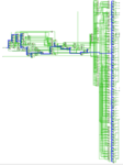
Just so you understand what I'm trying to convey here is the elaborated schematic of your code and the synthesized schematic

Elaborated HDL
Capture.PNG
Notice the enormous multiplexer that is circled on the left...

The Synthesized Version
Capture1.PNG
Clock network highlighted, but notice the large number of layers of combonational logic (the multiplexer from above).

Poorly written code means poorly implemented hardware. Learn to write hardware descriptions not programs. You wrote your code as if counter is the Program Counter of a microprocessor and you are bit banging the interface as you would in a microcontroller using GPIO. This is a terrible design. SPI is a serial interface so use a shift register and a FSM to control it.
 

thank you Sir ads-ee for your kind help and i am working on rectifying my errors(Shift reg and FSM). Sir FvM i am using digilent's spartan 3e kit which has Linear Technology's 2 channel 14 bit onboard adc in the kit. Could anyone tell me what is the optimum frequency for spi_sck i mean for both the amp and adc together if i give both of them the same serial clock.
 

thank you Sir ads-ee for your kind help and i am working on rectifying my errors(Shift reg and FSM). Sir FvM i am using digilent's spartan 3e kit which has Linear Technology's 2 channel 14 bit onboard adc in the kit. Could anyone tell me what is the optimum frequency for spi_sck i mean for both the amp and adc together if i give both of them the same serial clock.

The optimum clock is the slowest frequency clock of both devices. If you try to run any fater than that with a shared clock you will likely see errors.
 

Status
Not open for further replies.

Part and Inventory Search

Welcome to EDABoard.com

Sponsor

Back
Top