Continue to Site

Welcome to EDAboard.com

Welcome to our site! EDAboard.com is an international Electronics Discussion Forum focused on EDA software, circuits, schematics, books, theory, papers, asic, pld, 8051, DSP, Network, RF, Analog Design, PCB, Service Manuals... and a whole lot more! To participate you need to register. Registration is free. Click here to register now.

Transistor as a switch - Output current

Status
Not open for further replies.

brianfernandes

Newbie level 4
Joined
Aug 25, 2016
Messages
5
Helped
0
Reputation
0
Reaction score
0
Trophy points
1
Location
Pune, India
Activity points
75
I've been able to successfully use a 2n2222 transistor as a switch in my circuit, the switching part of which looks like the schematic below. My load is actually a **broken link removed** which takes the place of Rc in the above diagram. I've only activated one relay though, and this is still at the design stage, so I'm asking additional questions here so I can be sure this is a good long term design too.


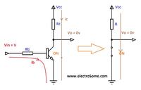
All articles on the "transistor as a switch" subject will recommend that Ib should be calculated using a variation of Ic / Hfe (ignoring gain curves, temp, etc.)

1) My first question is - why? Isn't the load being supplied from Vcc, and that's where Ic would be drawn from? The transistor itself is not amplifying Ib to produce Ic ... or is it? Not sure how I should be analyzing that circuit since it has two voltage sources.

2) Say Hfe is 100 and Ib is 0.5mA, then Ic = 100*0.5mA = 50mA. Suppose my load was drawing 100mA, what would happen? Would the transistor burn out or simply go off saturation and be inefficient?

3) The current drawn by my load is variable. Since it is a 4 channel relay, the current required depends on the number of relays activated. From what I know, it can vary from a little current required, to about 80 - 100mA (at 20mA per activated relay). If I do use the above calculations and design for an Ic that's say, 150mA (to be safe) - what would happen when my relays are inactive, would the current be wasted through the emitter and cause some heating there? How would this affect the lifespan of the transistor, and would this be an inefficient design (at least 70% of the time, the relays would be off).

I know these questions are rather fundamental, but unfortunately I've forgotten what little AC design I've learned at university. Any explanation would be appreciated.
Thanks!
 

Hi,

1) My first question is - why? Isn't the load being supplied from Vcc, and that's where Ic would be drawn from? The transistor itself is not amplifying Ib to produce Ic ... or is it? Not sure how I should be analyzing that circuit since it has two voltage sources.
The transistor is not "generating" Ic, this is correct. But the transistor "regulates" or "controls" Ic.
A transistor with low base current is in it's linear region. This linear region is good if you want to build an audio amplifier, for example.
But in your case you want the transistor to act as a switch. = "Saturated" region. To get low V_CE = low voltage loss = low power loss.
You force more current into the base to ensure the transistor operates not in the linear region. You overdrive the base somehow.
With a transistor as a switch Ic is limited by the load...Ic is the typical load current...

2) Say Hfe is 100 and Ib is 0.5mA, then Ic = 100*0.5mA = 50mA. Suppose my load was drawing 100mA, what would happen? Would the transistor burn out or simply go off saturation and be inefficient?
Yes. When you see the Hfe chart it is given for a relatively high V_CE. But you want low V_CE. When you extrapolate the chart for very low V_CE you will see Hfe is far below the 100.
Let's assume you drive your transistor with 0.5mA base current. Then maybe V_CE will be 3V. This means your relay operates with 3V less voltage.. maybe it doesn't even turn ON.
Transistor will become warm, maybe hot.
Additionally the Hfe of 100 is a "typical value". At a true transistor it may vary from 70...140. So V_CE will vary in a wide range. Relay voltage is not very predictable. Not what you expect from a reliable circuit..

To 3)
What will happen? See the transistor as a mechanical switch. As said above Ic is limited by the load (relays). So if you don't connect all relays, then Ic will be less, maybe 10mA. Even if you calculated your circuit for 150mA (which is correct) this current will never flow, it is not wasted.
But when calculated for 150mA, then maybe you use 15mA of base current....even if 1mA would be enough.
The 15mA of base current will flow, making 14mA useless, so you can say those 14mA are wasted. Power is dissipated mainly in the base resistor.
When the relays are OFF, then there is no base current, hence no collector current, no relay current. No dissipated and no wasted power.

Klaus
 
Klaus,

I appreciate the prompt and detailed response - I wanted to make sure I understood as much as possible before replying.

1) The transistor "regulates" Ic:
What is happening in this circuit finally makes sense - that the transistor is not generating Ic, but affecting/controlling it through V_CE. Thanks!

2) Continuing with my Hfe = 100 and Ib = 0.5mA assumption for the sake of calculations.

Are you saying that if my load was drawing 40mA, my transistor would be in saturation, with the minimal V_CE, but if my load was drawing 100mA instead, my transistor would not be in saturation and V_CE would be high (or at least, not at an efficient value) - reducing the voltage available to my load?

In other words, even though V_BE and Ib are constant, the current drawn by the load would affect whether the transistor is in saturation or not?

3)
When the relays are OFF, then there is no base current, hence no collector current, no relay current. No dissipated and no wasted power.
a) I'm afraid I couldn't understand this. Suppose the load was disconnected from my circuit (an open circuit where Rc is) - Ic would be 0, would this mean Ib is 0 as well, even though that section of the circuit is complete/closed?

b) Now, in my circuit, the relay board is in the output circuit (Rc in the schematic). And even when all relays are off, Ic might be very low, say 10mA, as you stated. So I guess at least this current would still be flowing as Ic and the full Ib (say 15mA) would be flowing as well?

4) I realize Hfe might be much lower than 100, and furthermore, each transistor will have different characteristics. How can I test, empirically, that my circuit is optimally running?
What I can think of is:
  1. Calculate a good starting point for Ib, say - 15mA using our calculations from earlier, and hence an appropriate Rb.
  2. Turn on all my relays so that the maximum current is drawn by the relay board - ensure that they are operating correctly, of course.
  3. Measure V_CE with a multimeter - it should be close to 0.3V. If significantly higher, reduce Ib by adjusting Rb and repeat.
Do these steps make sense?

Thanks again!
Brian.
 

The datasheet for almost every transistor lists its "Electrical Characteristics, On Characteristics, Collector-Emitter Saturation Voltage". For the 2N3904 it is a maximum of 0.3V when the load is 50mA and the base current is 5mA (1/10th) even though the minimum hFE (when it is not saturated) is 60 at 50mA.
 
Yes, the datasheet for mine (2n2222) says V_CE(sat) is 0.3 with Ib at 15mA and Ic at 150mA, looks like the same, 10 times multiplier that the 2N3904 has. And looks like to get 150mA current when all relays are on, which I do need, I would have to really drive the base at 15mA.

I'm still interested in the answers to my questions though, especially #2 and #4 -are my empirical testing steps correct?
 

Hi,
I'm still interested in the answers to my questions though, especially #2 and #4 -are my empirical testing steps correct?
I think yo refer to post#3:
#2: for me it doesn´t seem to be a question. I don´t know what to answer. What do you want to know?

#4: The procedure per se makes sense..but
Measure V_CE with a multimeter - it should be close to 0.3V. If significantly higher, reduce Ib by adjusting Rb and repeat.
--> You have to increase Ib.

****
Using the recommended values: for 150mA switching, with 15mA base current, the specified max. V_CE is 0.3V...
Mind the 0.3V is no typical value, but a max. value.... therefore I believe in the datasheet and don´t verify it. If I´d verify all the specifications of a datasheet I don´t need a datasheet at all.

But for sure you are free to verify it.

Imagine: What if you find out, that V_CE is higher than 0.3V?
* Either you made a mistake..
* or the bjt is defective..
But what´s the consequence then?

Klaus
 
Klaus,

I'll ask #2 differently: For my sheet, we have Ib = 15mA, Ic = 150mA at V_CE(sat). With Ib at 15mA, what would happen if my load were to draw more than 150mA? Would the transistor move into the active region instead of saturation?

#4 - thanks. I wanted to empirically test more for understanding, and I see your point about trusting the datasheet, of course. The other unknown is the current that's actually going to be drawn by the relay board - have not been able to find a decent spec sheet for it and so my 100mA load current assumption was based on 20mA that I found as the current for the component relays when they are activated.

My plan was to start at 15mA and see what the lowest base current I could get away with, while keeping the transistor in saturation. Which is why my plan was to ensure that with a higher Ib, the transistor really was in saturation and then lower Ib to figure out what was actually required by the circuit.

Thanks again!
Brian.
 

The base and collector circuits are essentially independant when using it as a switch, there is, within reason, no problem in increasing Ib beyond saturation to ensure the switch is fully 'on' (Vce minimized). The rule of thumb is to calculate Ib at maximum collector current then multiply the result by 10 to produce guaranteed saturation without Ib becoming excessively wasteful. It isn't a scientific calculation but a practical one in most situations.

As to what happens if Ib is fixed but you try to increase Ic, the transistor ceases to be saturated and Vce starts to increase. It almost certainly wouldn't enter a linear region but power dissipation is W = (Vce * Ic) and with both increasing the transistor will heat up quickly.

Brian.
 
Hi,

I'll ask #2 differently: For my sheet, we have Ib = 15mA, Ic = 150mA at V_CE(sat). With Ib at 15mA, what would happen if my load were to draw more than 150mA? Would the transistor move into the active region instead of saturation?
Because the datasheet says "max", not "typical" they surely have built in some safety margin. So I don´t think 151mA make a problem, but I think 300mA can cause a problem (--> linear region).
150mA/15mA is a hFE of 10. You can see in the datasheet that with increasing current the hFE drops. (even with 500mA and a 10V drop it is better than 35)
For 500mA and 1V drop hFE is still at least 10.

***
The other unknown is the current that's actually going to be drawn by the relay board
That´s not the problem of the datasheet. You should know the current. Otherwise you should use worst case values. Nobody of us can tell the current, therefore nobody can give a detailed answer.
So for more than 250mA you could use a hFE of 9 or so...

****
Why bother about 15mA when the relay current is a multiple of it?

If you have problems in sourcing the base current, then why don´t you use a mosfet instead of a bjt? --> about zero base (indeed "gate") current and less voltage drop..less heating.

Klaus
 
As to what happens if Ib is fixed but you try to increase Ic, the transistor ceases to be saturated and Vce starts to increase. It almost certainly wouldn't enter a linear region but power dissipation is W = (Vce * Ic) and with both increasing the transistor will heat up quickly.
Thanks, this is exactly what I was curious about.
Why bother about 15mA when the relay current is a multiple of it?

If you have problems in sourcing the base current, then why don´t you use a mosfet instead of a bjt? --> about zero base (indeed "gate") current and less voltage drop..less heating.
That's true, I never really thought about it that way. I don't really have a problem sourcing 15mA, just academically curious about the efficiency of this circuit.

Thank you both for your prompt responses - I do believe I know what to do now, and have far better understanding of the theory behind this.

Brian.
 

Think of the BJT only as a Ibe current controlled Rce resistance much lower than the input bias R.


Vce may start with a saturation voltage, Vs between 20 and 200mV depending design of transistor then Vce rises with pullup current Ic*Rce in a linear fashion.

Rce is the differential collector emitter resistance that is current controlled by Ib, when saturated.
Note that Rce is inverse to Ib when saturated.

RdsOn is similar in FETs except voltage threshold controlled.

Rbe is also effectively controlled by Ib but if Vce rises great than Vbe, it comes out of saturation gradually.

Typically you choose the max Vce.(sat) then decide what IC:Ib ratio to use between 50 and 10 low and high currents.

This ratio is device dependent and is often 10% of the linear hFE
 

Status
Not open for further replies.

Similar threads

Part and Inventory Search

Welcome to EDABoard.com

Sponsor

Back
Top