Continue to Site

Welcome to EDAboard.com

Welcome to our site! EDAboard.com is an international Electronics Discussion Forum focused on EDA software, circuits, schematics, books, theory, papers, asic, pld, 8051, DSP, Network, RF, Analog Design, PCB, Service Manuals... and a whole lot more! To participate you need to register. Registration is free. Click here to register now.

[moved] sinusoidal pulse width modulation inverter

Status
Not open for further replies.

maaxamed

Newbie level 6
Joined
Aug 4, 2016
Messages
13
Helped
0
Reputation
0
Reaction score
0
Trophy points
1
Activity points
140
Hello everyone I joined this blog last week I was really amazed at the work you put in the blog and attracted to be a member of this group.

Before I was going to ask a question I was reading of this website to find out how to build SPWM INVERTER.

like pure sine wave inverter up to page 8
Also I am a bit confused please can someone advise me were to begging.


many thanks.
 
Last edited by a moderator:
Re: sinusoidal pulse width modulation inverter

Sinewave inverters are a popular topic. Try a forum search on keywords of interest. Look through the list of related threads further down this column.

Have you built any type of inverter?
 
Re: sinusoidal pulse width modulation inverter

Sorry about the late reply,
I haven't built a inverter but..

I read the related threads and I got out of it that the starting point for someone relatively new is the ' push pull topology'. am a bit confused about the micro controller, does it need to be programmed or can it be analogue? Also between these SG3525, TL494, DBL494 which is the easier to use. And also I have programmable skills but what software is easy to simulate and program micro controllers?

Thank you
 

Re: sinusoidal pulse width modulation inverter

you start with expected outputs for V, I and wave shape( sine , square or 3 level or 5 level )and well defined inputs.
define intended application load.
then choose topology That works best.

If you are certain it is sine wave, then understand impedance transformation from load to source lowers by N squared and MOSFET RdsOn must be <= 2% of this for efficient operation.

Since cross-conduction of bipolar switches shorts out the supply, you need a dead-band in commutation of a few us or more. But when both switches are open, it raises source impedance of inverter.
 

Re: sinusoidal pulse width modulation inverter

After I looked and learnt the generation technique for sinusiodal PWM signal. The topology I have chosen was half-bridge bi-polar MOSFETs which is controlled by analogue op amps. The source I wanted to use is 12Volts lead acid batteries. I also looked into the dead time which can be controlled by programming to avoid the porblem of switch damage.

However is there an e-book on a practical method to create and test these parts. Is there a type of circuit/ project I am able to start on that will help me to fully test and understand the parts.

Lastly do I need to wind my own transformer to meet the specific criterias or are the any ready made ones.

Thank you
 

Re: sinusoidal pulse width modulation inverter

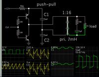
This is my impression of a push-pull step-up inverter. It probably is different from what you have in mind.

The transformer receives 1/2 of supply voltage. This forces you to double the step-up ratio, and the Amperes going through the primary. It probably is not the most efficient method.

To make sine PWM will be a further challenge.


A full H-bridge is a typical method for what you want to do.
 
Re: sinusoidal pulse width modulation inverter

Thanks for the reply

I will use the full h-bridge method and was wondering if you can provide steps to creating the sine pwm inverter from there and a recommendation for a suitable simulation software.

Secondly which project is better to try and create sine pwm inverter practically.

Thanks
 

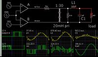
This is my simple simulation of a sine PWM inverter. It steps up 12VDC to 230 VAC. The op amps have two roles combined: (a) mimic a full H-bridge, and (b) generate sine PWM for the H-bridge.


This is not the circuit anyone would want to build. The switching frequency needs to be faster. Component values need to be adjusted accordingly.

This was done in Falstad's animated interactive simulator. Free to download and use. Your computer needs to have Java installed. It supports a few generic IC's. It does not contain the IC's you named (SG3525, TL494, DBL494).

www.falstad.com/circuit
 

Thank you for helping me, I appreciate it very much. I will now start on this and let you know how ill get on.
 

I applied the circuit above on falstad software and simulated it. I'm still studying the sine wave forms, but I was wondering about whether you could suggest a circuit with it haing a full h-bridge. Could this still be simulated on the falstad software or would it have another software as microchips might be applied to the circuit.

Thank you
 

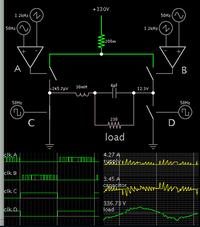
This simulation has the H-bridge with SPWM switching.


Notice the action resembles a buck converter in one direction, then another buck converter in the other direction. A lower switch conducts continuously to ground for 1/100 second (half a cycle). Only upper components need to do the rapid switching.

It is common for builders to choose a carrier frequency which is much faster than my simulation has.
 

Thanks for that, however I was wondering what the inputs were. The generators through the op amps are they connected or not. and what is the point of having such a high 330v input, what does it achieve?
 

This simulation has the H-bridge with SPWM switching.


Notice the action resembles a buck converter in one direction, then another buck converter in the other direction. A lower switch conducts continuously to ground for 1/100 second (half a cycle). Only upper components need to do the rapid switching.

It is common for builders to choose a carrier frequency which is much faster than my simulation has.
You know the options> timing > enter lower time resolution > then clocks can run faster than 25kHz default
right? It would be nice of you to share some of your fine simulations> files> export link> then here insert hyperlink
 

Thanks for that, however I was wondering what the inputs were. The generators through the op amps are they connected or not.

Behavior is simple as I could make it, simple as the simulator permits. The comparators (op amps) are 'cheating' because I set them to output positive waveforms only. It clarifies the SPWM waveform. I needed to try many adjustments of amplitude and polarity, both of the sine and sawtooth. It works in theory but it is not necessarily what you would do in hardware.

Notice you'll need several op amps to make:
* sine wave oscillator (50 or 60 Hz)
* inverted sine waveform
* sawtooth wave oscillator
etc.

To drive the H-bridge properly you'll need to decide what components to use, and how to bias them properly. Etc.

and what is the point of having such a high 330v input, what does it achieve?

330 is the peak of 230V sine. (Or else 170 is the peak of 120V sine.) You need to start somewhere in the vicinity of your desired peak voltage. My simulations above are not complete working schematics. They are overly simplified, so as to clarify concepts of operation.

There is an inverter topology which does it this way:
(1) chop 12V into high frequency AC sq waves
(2) feed it (high Amperes) to a step-up transformer
(3) rectify 330 V sq waves
(4) send 330V as SPWM (low Amperes) through H-bridge
(5) filter the output.

Or if you wish, you can do everything in one stage, namely feed 12V (high Amperes), through an H-bridge as SPWM to a transformer, and filter the high-V AC.
 

In a 3 phase inverter output line RMS is ( Vdc/2/√(2)) * √(3)...you can add another 15 -> 20% if you are using third harmonic injection.
 

You know the options> timing > enter lower time resolution > then clocks can run faster than 25kHz default

Yes this is essential to know. I was unaware of adjusting the timestep until someone told me about it. Seems odd that it wasn't made more prominent.

It would be nice of you to share some of your fine simulations> files> export link> then here insert hyperlink

Thanks, Tony. (I hope you're referring to my simulations.)

These links are for the previous two.

opamps mimic H-bridge 12V SPWM step-up xfmr LC filter 230VAC sine


In case my schematic does not appear in the website simulator, copy the list below and paste in the 'Import' window.


Code dot - [expand]
1
2
3
4
5
6
7
8
9
10
11
12
13
14
15
16
17
18
19
20
21
22
23
24
25
26
27
28
29
30
31
32
33
34
35
$ 1 1.1E-6 13.097415321081861 30 330.0 45
R 96 240 32 240 0 4 800.0 5.0 5.0 0.0 0.1
x 590 323 640 329 0 24 load
w 208 288 272 288 2
w 208 192 272 192 2
R 96 176 48 176 0 1 50.0 10.0 0.0 0.0 0.5
x 174 275 188 281 0 24 B
R 96 304 48 304 0 1 50.0 10.0 0.0 3.141592653589793 0.5
x 173 175 190 181 0 24 A
l 448 192 528 192 0 0.26 -0.21650951208107352
r 608 192 608 288 0 460.0
a 96 192 208 192 1 12.0 0.1 1000000.0
w 96 240 96 208 0
a 96 288 208 288 0 12.0 0.1 1000000.0
w 96 240 96 272 0
T 336 192 448 288 0 0.02 30.0 -5.306442231746243 0.21572657323807212 0.999
x 365 182 418 188 0 24 1:30
x 350 321 460 327 0 24 20mH pri
r 272 192 336 192 0 0.05
c 528 192 528 288 0 3.0E-6 -28.302425590033128
x 474 162 502 168 0 24 L1
x 539 272 571 278 0 24 C1
w 528 288 448 288 0
w 528 192 608 192 0
w 528 288 608 288 0
w 272 288 336 288 0
r 448 192 448 288 0 4600.0
o 3 128 0 34 16.36695303948071 20.94969989053531 0 -1 output A
o 2 128 0 34 17.498005798264096 22.397447421778043 0 -1 output B
o 17 128 0 33 1.093625362391506 44.79489484355609 1 -1 pri
o 25 128 0 34 489.88833106573423 0.03827252586451049 1 -1 sec
o 8 128 0 33 234.89251465925076 2.348925146592508 2 -1 L1
o 8 128 0 34 523.7424972633827 0.6546781215792284 2 -1 L1
o 18 128 0 33 279.96809277222553 1.3998404638611277 3 -1 C1
o 9 128 0 34 374.9852764287038 0.46873159553587984 3 -1 load


opamps SPWM 330VDC H-bridge EZ-switches LC filter 230VAC sine


Code dot - [expand]
1
2
3
4
5
6
7
8
9
10
11
12
13
14
15
16
17
18
19
20
21
22
23
24
25
26
27
28
29
30
31
32
33
34
35
36
37
38
39
40
$ 1 1.6999999999999998E-6 24.46919322642204 36 330.0 45
g 208 368 208 400 0
R 336 112 336 64 0 0 40.0 330.0 0.0 0.0 0.5
g 464 368 464 400 0
R 176 144 176 80 0 4 1200.0 1.3 3.7 1.5707963267948966 0.1
x 346 391 396 397 0 24 load
w 464 272 416 272 2
w 256 272 208 272 2
a 160 144 160 224 0 5.0 0.0 1000000.0
R 144 144 144 112 0 1 50.0 2.5 2.5 0.0 0.5
w 160 224 192 224 0
r 336 112 336 176 0 0.2
x 535 225 549 231 0 24 B
159 208 176 208 272 0 0.2 1.0E10
159 208 272 208 368 0 0.2 10000.0
159 464 272 464 176 0 0.2 1.0E10
159 464 368 464 272 0 0.2 10000.0
w 208 176 336 176 0
w 336 176 464 176 0
R 496 144 496 112 0 4 1200.0 1.3 3.7 1.5707963267948966 0.1
R 528 144 528 80 0 1 50.0 2.5 2.5 3.141592653589793 0.5
w 512 224 480 224 0
x 121 221 138 227 0 24 A
l 320 272 256 272 0 0.03 0.01524452075731987
r 416 352 320 352 0 460.0
c 320 272 416 272 0 6.0E-6 152.27444229298106
w 320 352 320 272 0
w 416 272 416 352 0
R 192 320 128 320 0 2 50.0 3.0 3.0 3.141592653589793 0.5
R 480 320 544 320 0 2 50.0 3.0 3.0 0.0 0.5
x 155 356 172 362 0 24 C
x 502 355 520 361 0 24 D
a 512 144 512 224 1 5.0 0.0 1000000.0
o 9 64 0 38 9.353610478917778 9.765625E-55 0 -1 clk A
o 20 64 0 38 8.749002899132048 9.765625E-105 0 -1 clk B
o 27 64 0 38 10.0 9.765625E-5 0 -1 clk C
o 28 64 0 38 10.0 9.765625E-5 0 -1 clk D
o 10 64 0 33 0.8949657474523425 9.16444925391199 1 -1 supply
o 24 64 0 33 279.96809277222553 11.198723710889022 1 -1 capacitor
o 23 64 0 34 598.6310706507378 0.7482888383134223 1 -1 load


Thanks very much for these explanations, it clarified what I was unsure about. Next time I will attach my circuit to a post.
 

To drive the H-bridge properly you'll need to decide what components to use, and how to bias them properly. Etc.

What are the best components that would go with the full h-bridge to create the best toplogy. It doesnt matter whether its analogue or digital.
thanks
 

Originally Posted by BradtheRad

''To drive the H-bridge properly you'll need to decide what components to use, and how to bias them properly. Etc.
i would like to see where the two following fit in to create a full circuit of H-bridge
1)opamps mimic H-bridge 12V SPWM step-up xfmr LC filter 230VAC sine
2)opamps SPWM 330VDC H-bridge EZ-switches LC filter 230VAC sine

secondly, What are the best components that would go with the full h-bridge to create the best toplogy
 

i would like to see where the two following fit in to create a full circuit of H-bridge
1)opamps mimic H-bridge 12V SPWM step-up xfmr LC filter 230VAC sine
2)opamps SPWM 330VDC H-bridge EZ-switches LC filter 230VAC sine

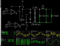
It starts getting complicated when we try to make the schematic more complete. This simulation has more components. The control circuitry is over-simplified. (It's plain to see the sine shape requires more adjusting.)


Making a simulation is easy compared to making a real inverter. There's the transformer design and construction. It's the heart of the inverter. If you wish to construct this project, it's wise to get experience building a square wave inverter first.
 

Status
Not open for further replies.

Part and Inventory Search

Welcome to EDABoard.com

Sponsor

Back
Top