Continue to Site

Welcome to EDAboard.com

Welcome to our site! EDAboard.com is an international Electronics Discussion Forum focused on EDA software, circuits, schematics, books, theory, papers, asic, pld, 8051, DSP, Network, RF, Analog Design, PCB, Service Manuals... and a whole lot more! To participate you need to register. Registration is free. Click here to register now.

[Moved]: for 6 bit ADC how to set the DAC parameter

Status
Not open for further replies.

madhusmita99

Newbie
Joined
Nov 18, 2013
Messages
3
Helped
0
Reputation
0
Reaction score
0
Trophy points
1,281
Activity points
1,311
Actually I am working on VCO based ADC in 180nm technology . I have some doubts related to that topic.

1.I am not getting the correct output after DAC when ramp and sine inputs are applied. so kindly let me know how u got the correct output

2. I have set the DAC (Vref=1,Vrise=0 ,Vfall=0,Vdelay=0,Vtran=.9)

3. I have set the clk frequency of 16.11 MHz .(vpulse period is 62ns and pulse width is 60ns) i.e reset signal to the counter

4. I have used ramp signal of duration 3.4u
(when time=0s, v1=1v
when time=3.4us, v1=400mv.). ADC count maximum when control volatge is .4vand minimum when voltage is 1v.
Kindly suggest the time duration of ramp so that i will get correct result.
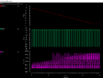
 

Need help related to the output after DAC

Can u send me the sample output of DAC when ramp and sine inputs are given to the ADC.
Whatever I have attached the output file , that one is correct or not . Kindly reply
 

Attachments

  • rampinput.png
    rampinput.png
    18.2 KB · Views: 134

Re: Need help related to the output after DAC

Hi,

It's not clear what you need.

Please post a complete specification. With vaues and units.

Klaus
 

How to set the ramp input parameter of ADC . so that it will give correct output.(I am getting the output as attached above )

Actually I am working on VCO based ADC in 180nm technology . I have some doubts related to that topic.

1.I am not getting the correct output after DAC when ramp and sine inputs are applied. so kindly let me know how u got the correct output

2. I have set the DAC (Vref=1,Vrise=0 ,Vfall=0,Vdelay=0,Vtran=.9)

3. I have set the clk frequency of 16.11 MHz .(vpulse period is 62ns and pulse width is 60ns) i.e reset signal to the counter

4. I have used ramp signal of duration 3.4u
(when time=0s, v1=1v
when time=3.4us, v1=400mv.). ADC count maximum when control volatge is .4vand minimum when voltage is 1v.
 

I fear, most Edaboard users don't know much about VCO based ADC. Posting a block diagram of your design would help to understand what you are asking.
 

Status
Not open for further replies.

Similar threads

Part and Inventory Search

Welcome to EDABoard.com

Sponsor

Back
Top