carsacc
Newbie level 1
Greetings everyone, currently i am working on my thesis and i am planning to use this IC (STA321MP) for my proyect as it fits the requierments that i am proposing for it, but there are some specific points and doubts that i can not solve along side the data sheet so that´s why i am writing this request. The questions goes as follows:
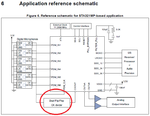
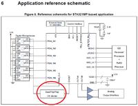
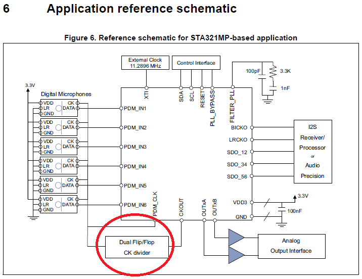
1) What is main function or porpouse of the Dual Flip Flop than can be seen in the image below? Is this one located inside the STA321MP or is and external component?
2) How does the PLL (phase locked_loop) ratio is program orr set? is not very clear on the data sheet.
3) What is the purpouse of the PLL_BYPASS pin ? Its functionality overall.
4) The subject around the PDM_CLK and how to obtain the CKOUT frequency is not very clear for me, could you please help me to understand it in a simpler way.
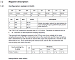
5) The sampling frequency that is said on the datasheet of the STA321P supports a 2.8224Mhz frequency with a internal fixed clock of 90.3168 hz, Is it a fixed default value? is it variable or i can be set apart?
Time is of scense for me, i would apreciate any help you can provide me. Thanks before hand.
Here is a link to the datasheet of the sta321mp:
https://www.st.com/content/ccc/resource/technical/document/datasheet/group3/f8/d2/89/64/7e/28/4d/11/DM00046002/files/DM00046002.pdf/jcr:content/translations/en.DM00046002.pdf
Good Day.
1) What is main function or porpouse of the Dual Flip Flop than can be seen in the image below? Is this one located inside the STA321MP or is and external component?
2) How does the PLL (phase locked_loop) ratio is program orr set? is not very clear on the data sheet.
3) What is the purpouse of the PLL_BYPASS pin ? Its functionality overall.
4) The subject around the PDM_CLK and how to obtain the CKOUT frequency is not very clear for me, could you please help me to understand it in a simpler way.
5) The sampling frequency that is said on the datasheet of the STA321P supports a 2.8224Mhz frequency with a internal fixed clock of 90.3168 hz, Is it a fixed default value? is it variable or i can be set apart?
Time is of scense for me, i would apreciate any help you can provide me. Thanks before hand.
Here is a link to the datasheet of the sta321mp:
https://www.st.com/content/ccc/resource/technical/document/datasheet/group3/f8/d2/89/64/7e/28/4d/11/DM00046002/files/DM00046002.pdf/jcr:content/translations/en.DM00046002.pdf
Good Day.