tiwari.sachin
Full Member level 6
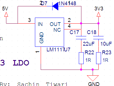
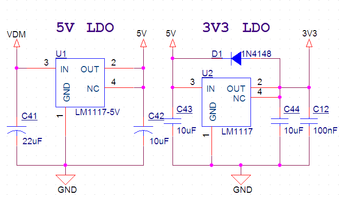
I am using 7.4V Li Ion Battery, followed by a 5V (1117) regulator, the output of which is given to 1117 (3.3V)
The input (Li Ion) voltage depending on load is flatuating (Dropping to say 6.8V).
I am connecting a bluetooth module also at 3.3V.
Observations
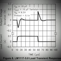
I closely looked and I saw that 3.3V drops 200-300mV (Approx) for about 7ms and comes back to 3.3V and some spikes (lots of up down lines on CRO) of few mV variations.
This I think is efefcting bluetooth throughput
How can i make sure that the voltage is stable
If I use a saparate supply only for bluetooth with common ground ofcourse, it works fine
The input (Li Ion) voltage depending on load is flatuating (Dropping to say 6.8V).
I am connecting a bluetooth module also at 3.3V.
Observations
I closely looked and I saw that 3.3V drops 200-300mV (Approx) for about 7ms and comes back to 3.3V and some spikes (lots of up down lines on CRO) of few mV variations.
This I think is efefcting bluetooth throughput
How can i make sure that the voltage is stable
If I use a saparate supply only for bluetooth with common ground ofcourse, it works fine