rfb2
Newbie level 3
Hi,
I ran across this in (original thread).
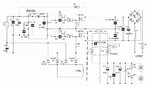
I'm familiar with simpler power supplies so I mostly understand the diode bridge connecting to the transformer and the rectification/filtering/zener occurring in the bottom right output stage.
There are a number of elements that I don't get and was hoping for some insight on:
1) From what I can tell the IR2153 just provides an alternating pulse to the 2 MOSFETs. What is the benefit of doing this pulsing action? Why does the output incorporate the caps C5 and C11? Just smoothing?
2) The C6/C12 structure splitting the transformer surprised me. I expected just a single cap value leading to ground for transients. Purpose?
3) L4 leading into the diode bridge. I'd never seen this before. Inductors impede AC. Don't we want this AC entering the transformer?
4) I see the use of the first MOSFET (T1). I don't understand T2. It seems to me current should always flow out the left side of the diode bridge. If T1 isn't on, there's no path for current to enter T2. From the IR2153 datasheet LO and HO (pins 5 and 7) are mutually exclusive. I must be missing something.
5) The lower left quadrant. Not sure what its purpose is or how he's getting 18v AC down there.
Appreciate any help you can provide. Thanks.
I ran across this in (original thread).
I'm familiar with simpler power supplies so I mostly understand the diode bridge connecting to the transformer and the rectification/filtering/zener occurring in the bottom right output stage.
There are a number of elements that I don't get and was hoping for some insight on:
1) From what I can tell the IR2153 just provides an alternating pulse to the 2 MOSFETs. What is the benefit of doing this pulsing action? Why does the output incorporate the caps C5 and C11? Just smoothing?
2) The C6/C12 structure splitting the transformer surprised me. I expected just a single cap value leading to ground for transients. Purpose?
3) L4 leading into the diode bridge. I'd never seen this before. Inductors impede AC. Don't we want this AC entering the transformer?
4) I see the use of the first MOSFET (T1). I don't understand T2. It seems to me current should always flow out the left side of the diode bridge. If T1 isn't on, there's no path for current to enter T2. From the IR2153 datasheet LO and HO (pins 5 and 7) are mutually exclusive. I must be missing something.
5) The lower left quadrant. Not sure what its purpose is or how he's getting 18v AC down there.
Appreciate any help you can provide. Thanks.