Continue to Site

Welcome to EDAboard.com

Welcome to our site! EDAboard.com is an international Electronics Discussion Forum focused on EDA software, circuits, schematics, books, theory, papers, asic, pld, 8051, DSP, Network, RF, Analog Design, PCB, Service Manuals... and a whole lot more! To participate you need to register. Registration is free. Click here to register now.

about choosing L for MOSfet

Status
Not open for further replies.

malhar

Newbie level 3
Joined
Aug 7, 2015
Messages
4
Helped
0
Reputation
0
Reaction score
0
Trophy points
1
Activity points
26
hello I am working on LNA design using TSMC 90nm CMOS process. the minimum L can be taken as 0.1 um but what is the maximum value of L that can be taken for CMOS. for eg, can i use the same model for L of 0.175 um or 0.3 um ???
 

In some cases you will find that the model makes up its
own mind about details based on L; even case-wise model
branches above and below some breakpoint. The foundry
modeling folks made that decision for you.

Or you may see NMOS devices "duplicated" with analog,
digital and RF transistors, each pointing to its own model
and with expected constraints on L, W, gate contacts
and so on, with differing tradeoffs in model accuracy /
complexity / solution speed (e.g. "digital" can be
expected to be minimum or near-minimum L, analog
longer L, RF minimum L with better gate contact rules
and maybe a narrower W limit, etc.).

In a LNA you almost never will want a longer than minimum
L (otherwise you are using too expensive a flow for the
frequency of interest).

PDK docs or the device properties form ought to constrain
the L values you can select by their callback functions.
 

But rf circuit design demands larger devices it's only for some transistors that you need minimum L for eg like feedback transistors but rest of the transistors like current sources etc requires devices with larger L
 

... can i use the same [L=0.1µm] model for L of 0.175 um or 0.3 um ?
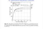
I'd think these lengths aren't so much longer that you couldn't use the min. length model. You can expect distinctly better (lower) gds (i.e. higher rds or VA) values for longer L, see e.g. the foll. figure for an Lmin=0.18µm process, which shows the CLM (channel length modulation) dependency on L :

gds_dependency_on_CLM__Binkley.png

Similar impacts on the δId/δVds transconductance arise from other short-channel effects as carrier velocity saturation (mobility reduction due to the longitudinal field), VFMR (vertical field mobility reduction) and DIBL (drain-induced barrier lowering), which all work in the same direction (but with less impact than CLM causes).

You could check these differences by displaying the Id vs. Vds characteristics for different channel lengths for your own process.
 

Status
Not open for further replies.

Part and Inventory Search

Welcome to EDABoard.com

Sponsor

Back
Top