Continue to Site

Welcome to EDAboard.com

Welcome to our site! EDAboard.com is an international Electronics Discussion Forum focused on EDA software, circuits, schematics, books, theory, papers, asic, pld, 8051, DSP, Network, RF, Analog Design, PCB, Service Manuals... and a whole lot more! To participate you need to register. Registration is free. Click here to register now.

MOS intrinsic gain, EE240, test circuit MOSFET with opamp and current source

Status
Not open for further replies.

AMSA84

Advanced Member level 2
Joined
Aug 24, 2010
Messages
577
Helped
8
Reputation
16
Reaction score
8
Trophy points
1,298
Location
Iberian Peninsula
Activity points
6,178
Hi guys,

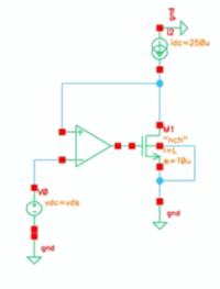
Has anyone tried to plot the gm.ro using the EE240 test circuit? That's the one I am talking about:


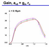
I think I have tried everything that I can think of. Didn't manage to get the results:


I know that this must be the small signal gain, but how to get around the above shown circuit was impossible for me. It's funny that even at the school where those slides belong, say how to do it.

It's simple frustrating.

Has anyone tried to get the gm.ro using this circuit?

Regards.
 
Last edited by a moderator:

What would you think is wrong with this relationship?
 

In first place I thought that this would't work, because you're forcing the current and by definition gm = did / dvgs. If id is constant gm is equal to zero. The same goes for the gds = did / dvds.

Even though I tried to simulate that circuit and I get a completly different plot:

gmgds.png

The devices I am using are 1.5V. I don't understand why I don't get the same curve. Anyway, to compare I have used another circuit where I put in the gate a vt+200mV vdc source and swept the Vds. I got the same thing.

Now I understand why every people that I asked if they know the gm/id method they say yes but never used. Maybe because either they don't know how to do this shi_t or just because they don't like it.

And from what I have heard, those guys in EPFL that offer courses on ic design, they all want to push people to do design using this method, but with no information around anywhere (I don't know if their course they teach properly how to design using this method) it's almost impossible.

Looks like people don't share the info because they don't want to teach people to design this way or to let them learn how to design better. Or maybe I am so fu*king dumb that I don't get how this shi_t works. Anyways.
 
Last edited by a moderator:

I don't see what makes gm respectively ro fall with Vds above 1.2V, except for specific transistor properties or hidden circuit features,
 
  • Like
Reactions: anhnha

    anhnha

    Points: 2
    Helpful Answer Positive Rating
Me neither. That's why I am asking.

Or those guys use their own transistor for teaching purpose or I don't know. We are talking about Berkeley. But they should specify that.

Some other docs I have seem at least one let's say, I think had the same behaviour.

If they hide things they shouldn't make available to people, although no one should rely on those stuffs.
 

You need to refer to the exact transistor model used with the exercise. I would expect that it's documented somewhere. You can see which parameter is causing the gain drop by looking at the internal model quantities over Vds variation.
 

I don't see what makes gm respectively ro fall with Vds above 1.2V, except for specific transistor properties or hidden circuit features,

It would be normal if the curve falls with Vds above 2V as ro decreases significantly with substrate current induced body effect.

- - - Updated - - -

Me neither. That's why I am asking.

Or those guys use their own transistor for teaching purpose or I don't know. We are talking about Berkeley. But they should specify that.

Some other docs I have seem at least one let's say, I think had the same behaviour.

If they hide things they shouldn't make available to people, although no one should rely on those stuffs.

Are you sure that this is 180nm process? If it is say 65nm process, the SCBE will be effective at lower voltage and reduces output resistance.
 

Status
Not open for further replies.

Part and Inventory Search

Welcome to EDABoard.com

Sponsor

Back
Top