Continue to Site

Welcome to EDAboard.com

Welcome to our site! EDAboard.com is an international Electronics Discussion Forum focused on EDA software, circuits, schematics, books, theory, papers, asic, pld, 8051, DSP, Network, RF, Analog Design, PCB, Service Manuals... and a whole lot more! To participate you need to register. Registration is free. Click here to register now.

Issues with Instrumentation Amplifier for Current Sensing

Status
Not open for further replies.

eengr

Member level 4
Joined
Mar 9, 2016
Messages
75
Helped
0
Reputation
0
Reaction score
0
Trophy points
1,286
Activity points
4,270
Hi all
I am using an instrumentation amplifier circuit to measure current on my jig.
Instrumentation amplifier has GAIN of 2. (See image below)
Instrumentation amp issues-no diode.jpg
Voltage diver (R124 & R125) at the output divides amplifier’s output by 2 so that Signal at ‘Current_sense’ is same as the voltage drop across 1R resistor hence same as current (ohms law V/R, R=1)
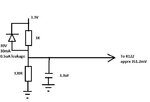
Current_Sense is connected to the input of a buffer (via MUX) and then to 24bit ADC (see the buffer & ADC circuit below)
Buffer and ADC.jpg

The circuit is used to measure current. At 1V Rail voltage and No load connected, R116 (sense resistor) has 0V drop across it BUT opamp-IC106 has apprx 9ish mV and then apprx 5mV at Current_sense.

When I connect a load so that R116 (sense resistor) has apprx 18mA, (Node with IC104 is more positive than Node with IC105 to show the load end) the Signal at Current_sens reads 18mA as well
So, it has an offset with No load condition but that is NOT reflected when there is a load connected.
I was wondering if someone could help me to understand what exactly is going on here and why I am getting offset with No load at input. Why this offset is not there when there is Load e.g., at 18mA and if there is a way to fix it so that I get ZERO at Current_Sense when No load is attached at input. Someone suggested to add an external diode at output of IC106 in the feedback path i.e., between pin 1 of IC106 and Node connecting R124 & R123 but not sure how that would help (as I tried it and with existing component values, it did Not work?

BOM is:
IC104, IC105, IC106 = OPA140 (from TI)
R116 =1R (1%) / 2512
R117 = R119 = R120 = R121 = R122 = R123 = 10K (0.1%) – 0603
R118 = 20K
R124 = R125 = 100K
Jig_Filtered_Supply = 9V

R280 = 1.5K
R281 = Not fitted
C207 = 1nF
D204 = D207 = 0.5uA leakage Schottkey Diode (Farnell-1459171)
IC215 = LTC2485 (24bit ADC)
 

Hi,

The problem is the lower supply rail, it is GND.
Every OPAMP has some dropout voltage to it's supply rails.
Some OPAMPS need some volts, yours is relatively good, there are only millivolts to the lower rail.

How to solve it:
Either you need a negative power supply fir the OPAMP, or -that's my preferred solution - you add some mV on the analog side and subtract the the equal value on the digital side.

Klaus
 
  • Like
Reactions: eengr

    eengr

    Points: 2
    Helpful Answer Positive Rating
Hi
thanks for the quick feedback.
I am bit confused here
You mentioned that problem is lower supply rail. The opamp is rated at 4.5V to 36V rail to rail output
I am operating it at 9V (well above minimum rated voltage)

It would be greatly appreciated if you could tell me how exactly is this 9V supply causing it to show 9ishmV output when there is NO voltage drop across Sense resistor (R116)
And why this 5mV not shown as offset at output when sense resistor has 18mV across it
 

Hi,

An opamp has two supply connections. In your case 0V for the lower rail and 9V for the upper rail.

The output can not completely to 0V nor to 9V, there is always a small gap.

Klaus
 

Hi thanks for the feedback,
Does this mean that with NO input applied at sense resistor (R116), I would have a non-zero output voltage due to intrinsic characteristics of any opamp?
Which parameter on datasheet would define this? Is it the offset voltage? For this amplifier it is given as 220uV (worst case). OR is the specs under the heading Voltage output? which is given as V(-) +0.35 to V(+) -0.35 (worst case)
If its later then does that mean I need to have at-least 375-400mV Reference voltage applied to the node of R122 which is currently connected to GND(0V)?
 

Your power demands will be modest; why don't you try to divide the 9V into -4.5V, 0V and 4.5V using a resistor divider and use that way? Unless, of course, there are other considerations...
 
  • Like
Reactions: eengr

    eengr

    Points: 2
    Helpful Answer Positive Rating
Hi,

Does this mean that with NO input applied at sense resistor (R116), I would have a non-zero output voltage due to intrinsic characteristics of any opamp?
It can not go exactely to the supply rails.
If one supply rail is 0V than the output can never be exactely 0v.

My opinion: This is no only for OPAMPs. This is the same for every loaded BJT, FET, analog switch.. any semiconductor... i´d even say: even for every hardware switch...
every semiconductor and every hardware switch will have a output resistance or contact resistance. Even if it is microohms, then there will be a voltage drop according Ohms law. U = R * I.
For a mechanical switch the difference may be in the microvolts, for fets in the millivolts and for BJTs in the tens of millivolts...

Which parameter on datasheet would define this?
This is quite straight forward:
* It is an "Electrical Characteristic" of the "Output".
Search the datasheet for "Electrical CharacteristiC" and you will come to Page 7, Chapter 6.7
Serach this chapter for "Output" and you will find a row (near the bottom of page 7) called "V_o Output Voltage"
(You already found this information)
And often there is a chart like "Figure 6". Here unfortunately it is only for supply rails of -18V and +18V.

***
does that mean I need to have at-least 375-400mV Reference voltage applied to the node of R122 which is currently connected to GND(0V)?
Correct!

***

Some comments about your circuit: (Forget about the folowing ... in case it causes confusion ;-))

--> The least-partcount-solution is to use a dedicated "current sense amplifier": Shunt + current_sense_amplifier + supply_capacitor. 3 parts.

****
If you want to use your OPAMPs, then i´d say (especially with your circuit) there is no need for the two OPAMPs of the first stage (IC104, IC105)
Use only the second stage = "difference amplifier" With IC106, R120, R121, R122, R123. Dont even use R124, R125.

The very small drawback of the reduced schematic is: A small - but known - offset of about 1V * 1Ohm / 20kOhm... wich is in the range of the OPAMP offset voltage.
But it is known, so you easily can compensate in software for that, if you like.
...oh yes, and a very low gain error is introduced, wich is far below your resistor tolerance errors. Also known ... and easy to compensate.
****

In either case: In my eyes it makes no sense to amplify a signal by 2 and then divide it by 2. This only creates new errors.

****
I wonder: usually one want very low voltage drop when measuring a current. Therefore usually R116 is in the milliohm region.


Klaus
 
  • Like
Reactions: eengr

    eengr

    Points: 2
    Helpful Answer Positive Rating
Thanks for detailed answer and it has been very helpful

I sent the part of schematic which I was having problems with.

In full schematic, the rail voltage is actually variable (controlled by controller) varying from 0V to 5V apprx (designed with OPAMP driving a NMOSFET much similar to what we see inside a LDO regulator. the feedback of output voltage is taken from Load side of sense resistor: (see picture below)
Full PSU.jpg


Current sense using instrumentation amplifier config is used to measure the current ranging from 0 to short circuit (As it is used to test a PCB, and before I apply full 4ishV across the PCB, I apply voltages in steps (starting from 0.5V apprx going up in 1V steps and measure the current to see if there is a short circuit at Load end. Normal operating current could be anything upto 0.7A
There is MAX9611 (3 parts solution - Shunt, current monitor and supply caps as you suggested) that could also be used to measure current, and I have used it in the past (with built in 12bit ADC), and I have used it here to limit the maximum current through circuit in feedback loop, but I wanted to compare the performance of MAX9611 against instrumentation amplifier (with 24 bit ADC) and see
which one gives better results. (NB: It is test kit one off so component count is not an issue)

Now, I know you mentioned to ignore your comments if they cause confusion BUT I am keen to know more about this (if you dont mind helping me with couple of things):

How did you calculate the offset of (1V *1 Ohm)/20k? There are plenty formuale in various text books but I learn and understand only when I actually hit a problem (which I have in this case)
Would the above number stay constant if the supply is varying for other cases (as mentioned above)?
Bit more on Gain Error please?
I wanted to avoid calibrating the jig for current measurement and be able to accurately measure current (0-0.7A) at processor end by putting the resistor values and worked out that the above resistor values would work but clearly if I need to connect something as Ref (375-400mV) on R122 then, I would need to consider changing sense resistor and Gain of Amplifier, BUT would that allow me to measure the current accurately to 0.1mA resolution (ideal) without calibrating the jig for current measurement by using an external DMM?
 

Hi,

How did you calculate the offset of (1V *1 Ohm)/20k? There are plenty formuale in various text books but I learn and understand only when I actually hit a problem
This offset is caused by the two 10k resistors across 1V. The current is 50uA. 50 uA on your 1 Ohms shunt causes 50uA.
It is not the offset of the OPAMP.

BUT would that allow me to measure the current accurately to 0.1mA resolution (ideal) without calibrating the jig for current measurement
No way.
Simple calculation: you use 0.1%resistors with a range of 1A...then the 0.1% make 1mA.
0.1mA accuracy: no. --> you need to calibrate.
0.1mA precision : yes. with careful design and well selected parts
0.1mA resolution: easily.

Klaus
 

The OP output diode is definitely wrong. The OP is required to sink current to achieve 0 output. Exactly zero output is impossible with a single supply OP. Preferred solution would be a slightly positive reference voltage, e.g. 0.1 V, substracted from the final output.
 
  • Like
Reactions: eengr

    eengr

    Points: 2
    Helpful Answer Positive Rating
Hi All, thanks for all the feedback and it has been very helpful to get insight of the circuit
Confused about the following: (pardon my ignorance on this topic but I want to get thorough understanding of the operation of this circuit)

Opamp's INPUT off set voltage
Opamp's Output offset voltage

Opamp's INPUT off set voltage (by definition as I understand) is he voltage that must be applied between the two input terminals of an OPAMP to null or zero the output. For OPA140, it is given as 220uV (worst case)

For the same OPA140, we DC output offset at ZERO as 350mV (worst case)

Now, when we discuss to compensate for offset, we refer to 350mV quantity and NOT the 220uV. I cant get my head around if there is a relation between these two quantities OR is it the word 'offset' causing this confusion?

Secondly, am assuming one or both of the aforementioned offsets vary with temperature. Would that mean that if my reference is set to 0V (as in first circuit without Diode), my ZERO value could be anything from 0 to 350mV?
Are we saying that by applying external reference voltage of 0.375 will put this circuit in a known controlled state? How?

Klaus,
The offset that you mentioned of 5V across 2x10K resistors. Am assuming these are R120, R122? When node of R122 is connected to a different reference as suggested e.g., 375mV, then, this drop will change? But, this circuit is at node of IC104's ouput where as current in 1R flows from IC104 to IC105 side (left to right) so, why would this current (through R120 & R122) cause a drop across 1R? With supply rail varying from 0.5V to 5V, would this mean that this factor will be different for each measurement? Would that mean different current calibrations for different rail voltage level?
 

Wrong term usage. 350 mV is no offset. It's output saturation voltage. It can't be compensated, you can avoid it's effect either by providing a bipolar supply voltage or shifting the zero reference point to a positive voltage, e.g. 0.5 V.
Are we saying that by applying external reference voltage of 0.375 will put this circuit in a known controlled state? How?
Yes. You'll connect the R122 foot point to a positive reference voltage and substract 0.5 V (or whatever the offset at the final ADC is) when processing the measured data.
 
  • Like
Reactions: eengr

    eengr

    Points: 2
    Helpful Answer Positive Rating
Thanks for the feedback. It clarifies the ambiguity caused by the term offset :)
Now, regarding the reference voltage application to opamp to compensate for the output saturation voltage, is it true for Buffer circuit as well?
As I have used buffer (at MUX output) just before the signal goes into the ADC (See attachment earlier)
The buffer is designed using AD8603 which could have output saturation of upto 50mV (for load of upto 1mA)
Some of the signals coming out of MUX are in the range of 15mV to 45mV.
Would I need a external ref greater than 50mV for buffer circuit as well?
How to get around that problem?
 

Hi,

Now, regarding the reference voltage application to opamp to compensate for the output saturation voltage, is it true for Buffer circuit as well?
You answered it by yourself. Yes.
The buffer is designed using AD8603 which could have output saturation of upto 50mV (for load of upto 1mA)

*****

Would I need a external ref greater than 50mV for buffer circuit as well?
Only one shift (by a reference voltage) is sufficent. It should be in front of the first AMP.

Klaus
 
  • Like
Reactions: eengr

    eengr

    Points: 2
    Helpful Answer Positive Rating
Only one shift (by a reference voltage) is sufficent. It should be in front of the first AMP.

Klaus

I have a 32:1 MUX and signals coming from various places from Unit under test and few of those signals are in range of 15mV to 50mV. MUX output goes to the buffer. which 'First AMP' you referring to?
 

Hi,

to prevent misunderstandings you could simply post your schematic.

Klaus
 
  • Like
Reactions: eengr

    eengr

    Points: 2
    Helpful Answer Positive Rating
Please see the attached full schematic

Jig is designed to test 4 different boards.
Signal to be measured are routed via 32:1 MUX and buffer to 24 bit ADC

On pp2 of schematic under the section S-Board3, there are some signals as:
Sn_B_PID_LMP_p6
Sn_B_PID_GAIN_p5

Both these signals at UUT (Unit Under Test) vary from 15mV (ish) to 13V.
Resistor divider is: R212=R214 = 100K / 0.1%
R213 = R215 = 10K / 0.1%

These signals go via 32:1MUX (IC216) (ADG731 from Analog devices) to the Net named MUX_OUT. R280 = 1.5K, C207 = 1nF. R281 = Not fitted
IC214 = AD8603 (opamp)
IC215 = LTC2485 (24bit ADC with full scale to 1/2 ref = 1.25V

Would this buffer be suitable to measure the signal at lower end ie., when Sn_B_PID_LMP_p6 = 15mV
D_Sn_B_PID_LMP_p6 = 1.3mV apprx (at buffer's input).
Buffer has Output saturation of apprx 50mV (at LOW level)
 

Hi there
I added an external reference of apprx 351.2mV to my instrumentation amplifier circuit (see the circuit below):
Reference voltage added.jpg

All the values of components are indicated in the picture above
I have also changed my sense resistor R116 to 0.5R
Problem:
When, my Rail voltage (variable supply voltage) changes, the voltage at reference at the node of R122 and new above newly added circuit changes. Changes in Rail has no effects on 3.3V rail that is used to generate the new reference. Few measurements taken:
Rail voltage Reference(at R122 node to 120R) Output of IC106 (opamp) (no diode)
0V 351.2mV 351.1mV
1V 356.4mV 356.44mV
2V 361.7mV 373.06mV
3.5V 369.8mV 373.06mV
4.2V 373.6mV 399.1mV

As it could be seen that with increase in Rail voltage the reference point starts moving
No load was connected on Rail (i.e., no current drawn through sense resistor)
Any idea why is this happening and how to fix it?

- - - Updated - - -

(Sorry last message was not formatted correctly)
Hi there
I added an external reference of apprx 351.2mV to my instrumentation amplifier circuit (see the circuit below):
Reference voltage added.jpg

All the values of components are indicated in the picture above
I have also changed my sense resistor R116 to 0.5R
Problem:
When, my Rail voltage (variable supply voltage that is used to test UUT) changes, the voltage at reference at the node of R122 and new above newly added circuit changes. Changes in Rail has no effects on 3.3V rail that is used to generate the new reference. Few measurements taken:

Rail voltage Reference(at R122 node to R_new2)Output of IC106 (opamp) (no diode)
0V351.2mV351.1mV
1V356.4mV356.44mV
2V 361.7mV373.06mV
3.5V369.8mV 373.06mV
4.2V373.6mV399.1mV


As it could be seen that with increase in Rail voltage the reference point starts moving
No load was connected on Rail (i.e., no current drawn through sense resistor)
Any idea why is this happening and how to fix it?
 

Attachments

  • Reference voltage added.jpg
    Reference voltage added.jpg
    16.9 KB · Views: 162

I see two different effects in the table.

1. The reference point is lifted according it's node impedance when it's loaded by the current through R120. Acts like increasing R122. You either need a buffered, really low impedance reference node or a reference voltage divider calculated into R122.

2. The OP output is even more lifted, at first sight not completely linear versus shunt common mode voltage. This suggests that 350-400 mV is still too high related to OP saturation voltage. The best test would be to supply the OP by a slightly negative V- and check if this problem disappears. There may be other, less obvious effects.

Another possible problem is resistor mismatch.
 
  • Like
Reactions: eengr

    eengr

    Points: 2
    Helpful Answer Positive Rating
Thanks for the feedback.
I have now added a buffer circuit for reference voltage with AD8603. I tried different reference voltages to check if things could be improved. See the schematic below:
Buffered Reference.jpg

No Load was connected at Instrumentation amp output, i.e., R124 & R125 disconnected to analyse the circuit in isolation. Sense resistor (R116) was set to 0.5R. Also, No load was conencted on variable supply rail i.e., NO current flowing through R116
Results obtained are:
Variable Supply RailBuffered Ref output OPAMP-IC106 outputOPAMP-IC106 (+) inputOPAMP-IC106 (-) input
0V429.7mV429.5mV219.3mV219.3mV
1V429.6mV429.6mV714.4mV714.7mV
2V429.6mV429.6mV1.2129V1.2134V
3.5V429.6mV432.9mV1.9622V1.9631V
4.2V429.6mV454.9mV2.32V2.321V

I replaced the OPAMP from OPA140 to OPA170 and they both showed same problem
I changed the OPAMP supply from 9V to 15V (to kill any chances of getting near Common Mode Voltage limit) but still the same issue.
I then changed the reference voltage to a higher value of apprx 814.5mV by changing R_new2
Results obtained as under:
Variable Supply RailBuffered Ref output OPAMP-IC106 outputOPAMP-IC106 (+) inputOPAMP-IC106 (-) input
0V814.5mV814.3mV411.7mV411.9mV
1V814.4mV814.4mV906.7mV907.1mV
2V814.5mV814.5mV1.4052V1.4058V
3.5V814.5mV817.9mV2.1546V2.1555V
4.2V814.5mV840.2mV2.5125V2.5137V

It could be seen that the reference is "stable" +/-0.1mV fluctuation in both cases (could live with that) BUT, the OPAMP output has a sudden jump when variable rail is changed from 2V to 3.5V and then to 4.2V
Any idea whats happening here and how to fix it.

(Cant use negative Rail, and all resistors are 0.1%)

- - - Updated - - -

Sorry guys,
Just found out that it even though NO external load was connected on Variable supply rail, there were three off 4.7V Zener diodes in parallel on this rail. these were taking current when rail jumped to 3.5V & then to 4.2V. I used them to protect the UUT to ensure that voltage never goes higher than 4.5V if software stops working. But did not realize that they would consume current even at 3.5V.
Removed those and now my OPamp output follows the reference voltage of 352mV linearly.
I assumed (and I know I should never assume in electronics testing) that there was no current through Rsense but in reality there was a small drop across it when Zener started conducting.
All fixed and sorted (hopefully :) )
Thanks for all the help
 

Status
Not open for further replies.

Similar threads

Part and Inventory Search

Welcome to EDABoard.com

Sponsor

Back
Top