Continue to Site

Welcome to EDAboard.com

Welcome to our site! EDAboard.com is an international Electronics Discussion Forum focused on EDA software, circuits, schematics, books, theory, papers, asic, pld, 8051, DSP, Network, RF, Analog Design, PCB, Service Manuals... and a whole lot more! To participate you need to register. Registration is free. Click here to register now.

Problems with substrate contact layout using IBM8HP

Status
Not open for further replies.

Chty

Newbie level 2
Joined
May 21, 2016
Messages
2
Helped
0
Reputation
0
Reaction score
0
Trophy points
1
Activity points
18
Hello All!
I was trying to draw a layout for a simple NPN in IBM8HP. Below is the schematic:
1.png
I used the "subc" as a contact to the substrate, which was provided by the PDK in the schematic. However, I don't know how to connect this "subc" in the layout!
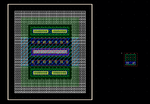
2.png
I didn't find the bulk terminal in the layout of the npn, but this bulk terminal appears in the schematic.

Could anybody please help??
Thank you very very very much!!!!
 

Didn't Virtuoso Layout XL show the connections as rubber-bands ??
 

Thank you so so so much for your reply!

No! I've tried to use the Virtuoso Layout XL in order to find some hints, but none was given.
There's another problem I am worrying about: Is it better for the substrate contact to form a guard ring in the layout? If so, I have to take the width and length of the substrate contact into consideration when designing the schematic, because I have to set the width and length of the "subc" symbol before placing it onto the schematic. I think it is hard for me to make sure what the length and width of the substrate contact would be before working on the layout of the whole circuit. :(
 

Status
Not open for further replies.

Part and Inventory Search

Welcome to EDABoard.com

Sponsor

Back
Top