Continue to Site
Follow along with the video below to see how to install our site as a web app on your home screen.
Note: This feature may not be available in some browsers.
Hi.., that you mentioned about frequency dependent capacitance ..
But i need Bias dependent capacitance, (How to plot Cgs vs Vgs ).
Rather I use AC analysis with AC_Vgs=1 and swept DC_Vgs.
Here Cg is evaluated by AC_Ig/(j*2*pi*freq).
What do you mean by cadence ?Than that i can find the capacitance from the location of "./kadi/filename/spectre/schematic/psf/dcOpinfo" folder from cadence.
I can not understand what you want to mean at all.But that too single capacitance value... with that how can i can plot .....?
What is "this tool" ?I am new to this tool

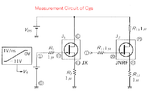
Driving gate-source by current is not appropriate.Follow my instructions in this image. Good luck.
Gate is floating.why not applying a step current to a capacitor and see voltage variations.
You can not understand Simulator at all.Why it is floating ?
EDA Tool Play is no more than Play.He is talking about ADS and plot,
you say measure with VNA? I do not get it.
I am talking about simulation not real world.
Than that i can find the capacitance from the location of "./kadi/filename/spectre/schematic/psf/dcOpinfo" folder from cadence. But that too single capacitance value... with that how can i can plot .....?
I hear too much gratuitous arbitrary statements in this thread...You can not understand Simulator at all
It is correct if initial condition is set.Although the gate is floating in the post #5 schematic with current source,
the transient analysis can well work by setting an initial condition for Vgs or skipping initial solution.
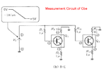
There is no problem in driving drain or source by current.(2) By measuring Igate with ramp wave Vgs drive.
This corresponds to Transient Analysis.
However it is difficult to estimate valid frequency range of Cgs.
You already agreed that it's possible to drive the gate with a current source if necessary prerequisites are met.There is no problem in driving drain or source by current.
However driving gate by current is not realistic.
No.Furthermore, there are real MOSFET circuits with a (in a first order) current driven gate, supplemented by a means that sets the DC bias.
There is a problem in an initial behavior for current step stimulus.But driving the gate by a current step or a voltage ramp are only different ways to stimulate the simulation
MOS Model Levle-1,2,3 give fairly different results between AC and Transient Analysis.If Cgs is only weakly frequency dependent,
the measurement in transient analysis will give almost the same result that a parametric small signal AC measurement with Vgs variation.
Transistor models say it's controlled by Vbe...BJT is a current controled device.
Bias is set by Ib not Vbe.Transistor models say it's controlled by Vbe...