jcv65
Newbie level 1
I am working on a project that interfaces an AD7626 Evaluation board to a Xilinx ARTIX FPGA (the FPGA is in a NEXYS VIDEO board from Digilent). I am having problems meeting the timing requirements of my design.
I am working in the Vivado Webpack development environment. My design is built around the Microblaze softcore processor and my interfacing between modules is done via the AXI buses and protocol.
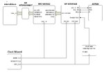
The AD7626 is an ADC and it interfaces with the host via 3 sets of LVDS lines: CLK, DCO and D(ata). The image below shows the block diagram with the module I created in Verilog interfacing with the AD7626

Note that MY_INTERFACE receives 3 clocks: The AXI_CLK (to interface with the rest of the modules in the microblaze based design, the ADC_CLK (in the diagram I call it CLK_FOR_ADC) and the DCO_CLK, (the last two are related as indicated below) The AXI_CLK and the ADC_CLK may have different frequencies, but in general they should be about the same order of magnitude. My biggest problem right now is how can I safely constrain the DCO_CLK and how to ensure my clock domains crossing are safe too.
The adc_sr_clk is a train of 16 pulses at the same frequency and in phase with ADC_CLK. This is used to extract the digitized data in serial form from the AD7626 shortly after it received the CNV (convert or digitize) pulse. The buffers BUFG, IBUFDS etc.are used to convert from LVDS to the levels used inside the FPGA.
Below is the timing diagram of the AD7626 signals. Note that the DCO_CLK signal is delayed from the CLK signal by 1/4 of a period, and that the middle of the data "eyes" is aligned with the rising edge of DCO_CLK

I used a Clock_wizard to generate the AXI_CLK (100MHz) and the ADC_CLK (100MHz). I understand that Vivado will create automatically determine that these two will be generated clocks (derived from the board'clock: 100MHz). To constrain the DCO I first created a clock with the timing wizard
create_clock -period 10.000 -name dco_clk -waveform {0.000 5.000} [get_ports dco_clk_p]
Then to indicate that DCO_CLK was delayed from ADC_CLK by about 1/4 of a period (2.5ns) I used the set_clock_latency constraint
set_clock_latency -clock [get_clocks dco_clk] -source -early 2.300 [get_ports dco_clk_p]
set_clock_latency -clock [get_clocks dco_clk] -source -late 2.700 [get_ports dco_clk_p]
---------------------------------------------------------------------------------------------------------------------------------------------
MAIN QUESTION
Could someone please tell me if I am doing this constrining correct? The timing analyzer fails:there is a Hold timing problem between the ADC_CLK and the AXI_CLK, but both clocks run at the same frequency and since they originate from the same CLK_WIZARD block they should have teh same phase.
I also have timing problems with teh oserdes_clk to oserdes_clkdiv I do not have an idea of what this error means, I am not familiar with the oserdes...
Thank you
--------------------------------------------------------------------------------------------------------------------------------------
Below is a rough block diagram of my overall system

I am working in the Vivado Webpack development environment. My design is built around the Microblaze softcore processor and my interfacing between modules is done via the AXI buses and protocol.
The AD7626 is an ADC and it interfaces with the host via 3 sets of LVDS lines: CLK, DCO and D(ata). The image below shows the block diagram with the module I created in Verilog interfacing with the AD7626

Note that MY_INTERFACE receives 3 clocks: The AXI_CLK (to interface with the rest of the modules in the microblaze based design, the ADC_CLK (in the diagram I call it CLK_FOR_ADC) and the DCO_CLK, (the last two are related as indicated below) The AXI_CLK and the ADC_CLK may have different frequencies, but in general they should be about the same order of magnitude. My biggest problem right now is how can I safely constrain the DCO_CLK and how to ensure my clock domains crossing are safe too.
The adc_sr_clk is a train of 16 pulses at the same frequency and in phase with ADC_CLK. This is used to extract the digitized data in serial form from the AD7626 shortly after it received the CNV (convert or digitize) pulse. The buffers BUFG, IBUFDS etc.are used to convert from LVDS to the levels used inside the FPGA.
Below is the timing diagram of the AD7626 signals. Note that the DCO_CLK signal is delayed from the CLK signal by 1/4 of a period, and that the middle of the data "eyes" is aligned with the rising edge of DCO_CLK

I used a Clock_wizard to generate the AXI_CLK (100MHz) and the ADC_CLK (100MHz). I understand that Vivado will create automatically determine that these two will be generated clocks (derived from the board'clock: 100MHz). To constrain the DCO I first created a clock with the timing wizard
create_clock -period 10.000 -name dco_clk -waveform {0.000 5.000} [get_ports dco_clk_p]
Then to indicate that DCO_CLK was delayed from ADC_CLK by about 1/4 of a period (2.5ns) I used the set_clock_latency constraint
set_clock_latency -clock [get_clocks dco_clk] -source -early 2.300 [get_ports dco_clk_p]
set_clock_latency -clock [get_clocks dco_clk] -source -late 2.700 [get_ports dco_clk_p]
---------------------------------------------------------------------------------------------------------------------------------------------
MAIN QUESTION
Could someone please tell me if I am doing this constrining correct? The timing analyzer fails:there is a Hold timing problem between the ADC_CLK and the AXI_CLK, but both clocks run at the same frequency and since they originate from the same CLK_WIZARD block they should have teh same phase.
I also have timing problems with teh oserdes_clk to oserdes_clkdiv I do not have an idea of what this error means, I am not familiar with the oserdes...
Thank you
--------------------------------------------------------------------------------------------------------------------------------------
Below is a rough block diagram of my overall system
