Continue to Site

Welcome to EDAboard.com

Welcome to our site! EDAboard.com is an international Electronics Discussion Forum focused on EDA software, circuits, schematics, books, theory, papers, asic, pld, 8051, DSP, Network, RF, Analog Design, PCB, Service Manuals... and a whole lot more! To participate you need to register. Registration is free. Click here to register now.

Layout critique LT3741 DCDC Buck Converter

Status
Not open for further replies.

Chuleo

Newbie
Joined
Mar 28, 2014
Messages
4
Helped
0
Reputation
0
Reaction score
0
Trophy points
1,281
Activity points
1,361
Hello everyone!

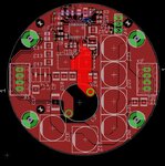
I'm a junior electrical engineer who got the task to design a constant current source. Since I'm not really experienced in PSU design I'd like you to
criticise my layout.

The schematic is basically the same as the one on the first page of the Datasheet: http://cds.linear.com/docs/en/datasheet/37411ff.pdf

Specs are: Input 30-36V, Output around 28V @ 15A. The converter will be used to pulse a load. Duty cycle will be approx 30% (1s on, 2s off) or less.

Input caps: 6x 10uf 1210 X7R/50V parallel. Output: 6x 120uf Aluminium polymer, low ESR 35V. Inductor saturation at 20A.

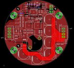
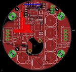
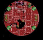
I tried to make all critical loops as small as possible. Not shown is the bottom layer (Ground pour except under the inductor) and the vias nailing the top ground pour and pads to the bottom ground plane.
The PCB will have 2 layers,70u copper and is 60mm diameter.

Have I made any big mistakes?

Thanks!

3.JPG

4.JPG

2.JPG

1.JPG
 

Hi,

I don´t see big mistakes.

You didn´t showthe vias from TOP_GND to BOTTOM_GND. They are important. I think it´s a good idea to show us.

Why that large output capacitor(s)?

Especially when you say it is switched ON/OFF in second ´s timing.
* Every time you need to charge the big capacitors
* and every time when it is switched OFF they are discharged and the energy is pushed back to the input. Expect overvoltage at the input!
(this is not the case when you DISABLE the switching controller, but then the output voltage won´t go down)

Klaus
 

Not sure if you defined properly the keepout distances. For instance, there is a track too close of the left edge of the board, which could be reached in the cutting process. In addition, the big SMD capacitors seems also as being too close, at least at first sight.
 

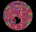
Here's a picture with the vias. Is it too much?

5.JPG

I expressed myself incorrectly, the load is meant to be switched. The DCDC converter will stay on. I forgot to mention, the switching frequency will be 500kHz.
I added the big capacitor because the datasheet states: "A minimum of 20uf/A load current should be used in most designs" so the minimum would be 300uF.

The DRC File is from the manufacturer, so i guess it should be ok. But you are correct, there are two traces that are quite close to the edge. I will move those. Or do you mean the spacing between the caps?

About the cap placement: I placed it there because in the datasheet it states "The input capacitor should be sized at 4μF for every 1A of output current and placed very close to the high side MOSFET"
 

Hi,

if you use the current limiting feature with your load, then expect the output voltage to rise with disconnected load.

You took care of the "increased" voltage when you switch ON the laod?
(It depends on the load. A LED doesn´t want those high current pulses (caused by discharging the capacitors), for a heating element or peltier element it won´t be a problem)

Klaus
 

Looks good at first glance. But it seems you've put vias underneath the controller's bottom pad. Have you taken measures to ensure that they won't steal solder from that pad?

If you plan on having it mass assembled, you may have trouble with large thermal gradients due to the large components clustered to one side. Also I hope you've properly estimated the temperature rise in the FETs and inductor?
 

Here is pcb layout guide doc
 

Attachments

  • Basics of SMPS Layout _4.doc
    645.5 KB · Views: 102

@treez

Thank you for that guide!

@mtwieg
There are only 5 vias under the LT3741 that could steal the solder, so I guess it wont bee too much of a problem. Since its a first prototype I can still change it if it becomes an issue.

It will eventually be assembled in a serie but not mass produced. I will talk to the fab house wheter they can do it or not. Yes I considered the thermal losses int he FETs and the inductor.
 

dont they tent the vias on the bottom side to stop solder being stolen? By tent i mean, having solder resist pasted over the via hole and annulus on the bottom side.
 

They do. But from what i heard it's far from optimal to have the via tented on the bottom side. It should be better to have it plugged, but that adds quite a bit to the manufacturing costs. Thats why I want to test it with a couple vias and see how it goes.
 

Status
Not open for further replies.

Similar threads

Part and Inventory Search

Welcome to EDABoard.com

Sponsor

Back
Top