Continue to Site

Welcome to EDAboard.com

Welcome to our site! EDAboard.com is an international Electronics Discussion Forum focused on EDA software, circuits, schematics, books, theory, papers, asic, pld, 8051, DSP, Network, RF, Analog Design, PCB, Service Manuals... and a whole lot more! To participate you need to register. Registration is free. Click here to register now.

Mux Synchronizer on Verilog FPGA

Status
Not open for further replies.

Samuel Jimenez

Newbie level 3
Joined
Oct 23, 2014
Messages
4
Helped
0
Reputation
0
Reaction score
0
Trophy points
1
Activity points
32
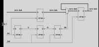
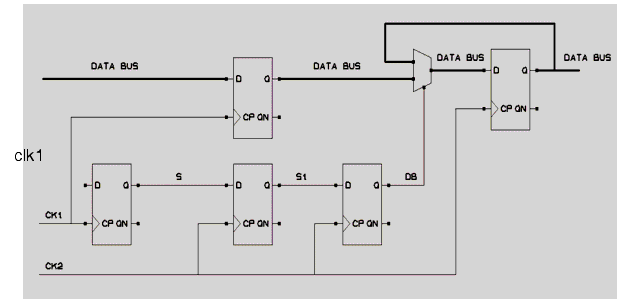
I need help implementing a mux synchronizer on Verilog. I have little knowledge of Verilog and need this design as soon as possible.


Any help is appreciated tremendously!!
 
Last edited by a moderator:

So is this your homework?

hint1:

Code Verilog - [expand]
1
2
3
4
// flip-flop code
always @(posedge clk) begin
  q <= d;
end


hint2:

Code Verilog - [expand]
1
2
3
4
5
6
7
8
9
10
11
// case mulitplexing
always @* begin
  case (sel)
    0       : mux_out = i0;
    1       : mux_out = i1;
    default : mux_out = 'bx;
  endcaes;
end
 
// ? : multiplexing
assign mux_out = sel ? i2 : i0;

Thank you,

No, it's not. I'm just having trouble how to appropriately interconnect mux output to the instantiated modules:

For ex, using your presented logic (not complete mux sync design - just an example):

Code:
cdc_dff dff1(
 //.input(..) D
 //.clk(..)   clk
 //.outout(wire) 
);

//then

cdc_mux mux_1 (
 //.mux_i0 (select_0),
 //.mux_i1 (select_1),
 //.mux_select (wire from dff1 output)
 //.mux_o (bus wire)
);

//then

always @(posedge dest_clk)
begin
    adc_a <= bus wire from mux_1;
end

Is this correct/appropiate?
 
Last edited:

No, it's not [homework].
:) glad to hear that...

I'm just having trouble how to appropriately interconnect instantiated modules:
Okay then...
I'm not exactly sure what you wrote it looks all wonky to me. Everything is commented out and none of the names match what I wrote above.
For ex (using your presented logic):

Code:
cdc_dff dff1(
 //.input(..) D
 //.clk(..)   clk
 //.outout(wire) 
);

//then

cdc_mux mux_1 (
 //.mux_i0 (select_0),
 //.mux_i1 (select_1),
 //.mux_select (wire from dff1 output)
 //.mux_o (bus wire)
);

//then

always @(posedge dest_clk)
begin
    adc_a <= bus wire from mux_1;
end

Is this correct?

just looking at the right two components the FF and the mux you would have to first change my code snippets to modules:

Code Verilog - [expand]
1
2
3
4
5
6
7
8
9
10
11
module flip_flop (
  input clk,
  input d,
  output reg q
);
 
  // flip-flop code
  always @(posedge clk) begin
    q <= d;
  end
endmodule


taking liberty with the names on your schematic, you have names that are identical for the data_bus for multiple connections.
with both this flip_flop file and the other mux code turned into a module will allow you to code something like this:

Code Verilog - [expand]
1
2
3
4
5
6
7
8
9
10
11
12
13
14
15
16
17
18
19
genvar i;
  generate
  // generate an 8-bit data bus
  for (i=0; i<8; i=i+1) begin : GEN_BUS
    // mux instance
    mux mux_i (
      .i0 (data_bus_fb[i]),
      .i1 (data_bus_in[i]),
      .sel (db),
      .mux_out (data_bus_o[i])
    );
    // FF instance
    flip_flop flip_flop_i (
      .clk (clk),
      .d (data_bus_o[i]),
      .q (data_bus_fb[i]) // feedback to mux input.
    );
  end
  endgenerate


Though I would never code anything with this type of structural description, why waste the time instantiating all of these tiny modules, just write behavioral code for the whole thing in like 20-30 lines of code (just a guess).
 

What is the point with proper synchronization for the mux select signal but not for the data path?
 

What is the point with proper synchronization for the mux select signal but not for the data path?
I think the MUX select is actually something like a data valid strobe. It's synchronized more to delay it than anything else. This allows the data to become stable. If you synchronize the data bus then you'll end up capturing garbage data every time as some bits may get transferred and some might get missed.

The circuit only works if the data and strobe changes only occur approximately every 3-4 destination clock cycles. Any faster and you'll end up coruppting some of the data transfers.
 
I changed to behavioral like so:
Here's the Verilog Code:

Code:
reg [16-1:2] a_a1_o, a_b3_o;
reg a_b1_o, a_b3_o;
reg a_mux_enable;

reg [16-1:2] b_a1_o, b_b3_o;
reg b_b1_o, b_b3_o;
reg b_mux_enable;

always @(posedge adc_clk_in)
begin
    a_a1_o <= adc_dat_a_i[16-1:2];
    b_a1_o <= adc_dat_b_i[16-1:2];
end

always @(posedge adc_clk)
begin
    if (a_mux_enable)
        a_b3_o <= a_a1_o;
    if (b_mux_enable)
        b_b3_o <= b_a1_o;
end

always @(posedge adc_clk)
begin
    a_b1_o <= adc_clk_in;
    a_mux_enable <= a_b1_o;
    
    b_b1_o <= adc_clk_in;
    b_mux_enable <= b_b1_o;

    //adc_dat_a <= data_bus_fb[16-1:2];
    adc_dat_a <= a_b3_o[16-1:2];
    adc_dat_b <= b_b3_o[16-1:2];
    
end

The circuit only works if the data and strobe changes only occur approximately every 3-4 destination clock cycles. Any faster and you'll end up coruppting some of the data transfers.

It seems this CDC may not be appropriate for my situation, then. Continuous multi-bit stream data is coming in (not bursts). What other CDC techniques might satisfy this requirement.
 

Use an asynchronous FIFO.
 

Use an asynchronous FIFO.

But the adc data stream is not ordered. I mean, with adc datastream that is not ordered, an async. FIFO with gray code counters would not work.

Or are the gray code counters only responsible for handling the writing/reading pointers?
 

But the adc data stream is not ordered. I mean, with adc datastream that is not ordered, an async. FIFO with gray code counters would not work.

Or are the gray code counters only responsible for handling the writing/reading pointers?

They are used to transfer the pointers across the clock domain...single bit changes in a multi-bit bus can be transferred without glitches in the counter order.

The FIFO data is still in a "First-In-First-Out" order, hence the name FIFO. So as each sample from the ADC is written to the FIFO on one clock domain the reading of the data on another clock domain comes out in the same order that the ADC generated the data.
 

Status
Not open for further replies.

Similar threads

Part and Inventory Search

Welcome to EDABoard.com

Sponsor

Back
Top