Alloy
Advanced Member level 4
Hey
Can anyone suggest me how to improve this PCB layout?
The transformer is 12V and logic side is working at around 200kHz.
The power side is at mains voltage and also works at around 200kHz.
The two MOSFETs will be placed on heatsink.
Please take a look:
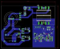
I did not make a single big ground polygon because I want mains ground to be separated from logical 12V ground.
Suggestions?
Can anyone suggest me how to improve this PCB layout?
The transformer is 12V and logic side is working at around 200kHz.
The power side is at mains voltage and also works at around 200kHz.
The two MOSFETs will be placed on heatsink.
Please take a look:
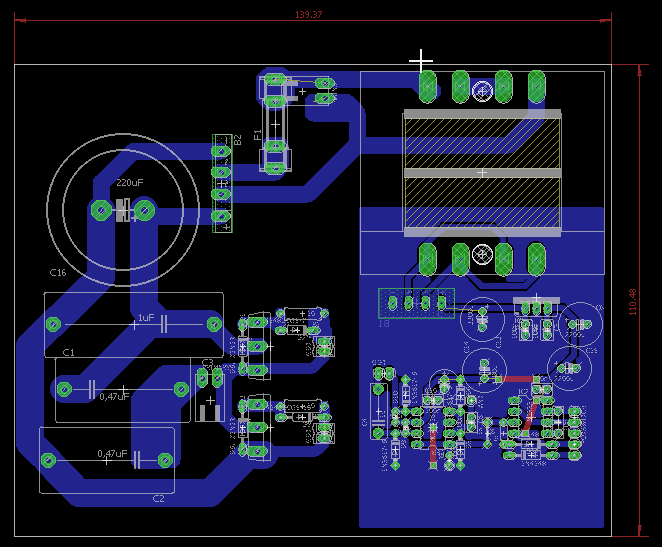
I did not make a single big ground polygon because I want mains ground to be separated from logical 12V ground.
Suggestions?