Continue to Site

Welcome to EDAboard.com

Welcome to our site! EDAboard.com is an international Electronics Discussion Forum focused on EDA software, circuits, schematics, books, theory, papers, asic, pld, 8051, DSP, Network, RF, Analog Design, PCB, Service Manuals... and a whole lot more! To participate you need to register. Registration is free. Click here to register now.

Very Simple audio amplifier design experiment

Status
Not open for further replies.

paulmdrdo

Full Member level 3
Joined
Jan 17, 2014
Messages
183
Helped
1
Reputation
2
Reaction score
2
Trophy points
18
Activity points
1,394
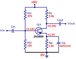
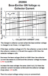
Hello! I am trying to do an experiment on building a simple audio amplifier using transistors. In particular I would like to use a 2n3904 trannie. But Im still not sure on what Am I going to base the dc operating point of my circuit. Do I just choose it randomly? I tried to consult the datasheet but i dont know what parameters in there I should base my operating point. Please help me. I know the math but i dont know what values to use in designing. Especially the hfe im not sure what to use.

Thanks!
 

The key is to find a proper operating point for the transistor. You need to adjust things so the output voltage swings inside a middle range between the supply rails.

Attach a potentiometer (say, 50k) to the bias terminal. Dial bias current up or down, to shift the output voltage up or down, until your audio signal comes through clearly. Of course this is just one thing that needs to be right about your circuit, in order for it to work.

- - - Updated - - -

At all times it's a good idea to touch a finger to the transistor, in case it heats up.
 

Hi,

audio amplifier..

You talk about only one transistor..
Do you really want a single transitor solution?

For sure it is possible, but sound quality, output power, power dissipation... may be critical.

****
If you show us a schematic we can better assist you, because we can "name" the parts.

Klaus
 

I would start choosing a DC quiescent current of some milliamps (1...5 mA).
Select an emitter resistor RE (very important!) which produces (for the selected current) a DC voltage of app. 10%...20% of the supply voltage Vcc..
The DC drop across the collector resistance RC should be app. 30%...40% of Vcc. The rest of the DC voltage gives the necessary collector-emitter voltage VCE.
Select some kOhms for the base voltage divider which must produce a voltage at the base node which 0.7 V above the DC potential of the emitter node.
Don`t care about current gain hfe.

EDIT: Don`t be disappointed, the circuit will have a rather low voltage gain (app. RC/RE) but it will have a very good DC stabilization.
You can increase the gain by placing a capacitor across RE (the value of CE must be large enough to short RE for the operating frequencies).
 
Last edited:

A single transistor amplifier design is never done randomly, it is simply calculated from a few simple rules and a few spec's from the datasheet.
1) Select a power supply voltage of maybe 9V and if the load resistance is very high then select a current for the transistor of maybe 1mA.
2) The base-emitter voltage of about 0.65V at a collector-emitter current of 1mA is different with each transistor and it changes when the temperature changes so an emitter resistor is used to reduce the variation in current caused by the differences.
3) Select a few times the base-emitter voltage to be across the emitter resistor so it will be about 1.5V. Then the emitter resistor is 1.5V/1mA= 1.5k.
4) You want the collector to swing equally up to +9V and down to almost +1.5V so it will be biased at halfway which is +5.25V.
5) The collector voltage is +5.25V so the collector resistor has 9V - 5.25V= 3.75V across it and has a current of 1mA so its value is 3.75V/1mA=3.75k ohms which is not a standard value, use 3.9k ohms.
6) The hFE is the DC current gain and the datasheet shows about 85 at 1mA printed in the datasheet spec's. Then the base current is about 1mA/85= 11.8uA. Select a current of 10 times for the voltage divider that biases the base. The base voltage is about 0.64V plus the 1.5V emitter voltage so it is 2.14V and the current in the voltage divider is 11.8uA x 10= 118uA.
7) The upper resistor of the voltage divider has 118uA plus the base current of 11.8uA so its current is 129.8uA and it has 9V - 2.14V= 6.86V across it so its value is 6.86V/129.8uA= 52.9k which is not a standard value, use 47k.
8) The lower resistor in the voltage divider has a current of 118uA minus the base current of 11.8uA so its current is 105.2uA and its value is 2.14V/105.2uA= 20.3k which is not a standard value, use 15k.

A capacitor is connected parallel to the emitter resistor to increase the voltage gain but the distortion at high level is also increased. If an emitter capacitor is not used then the base voltage must be a little lower to allow the emitter voltage to swing up a little when the collector swings down.
 

Attachments

  • transistor.png
    transistor.png
    9.2 KB · Views: 70
Audioguru, that was an exceptional post.
 

I simulated the circuit using a "typical" 2N3904 transistor to show you the difference in voltage gain and distortion with and without an emitter capacitor:
 

Attachments

  • transistor1.png
    transistor1.png
    43.6 KB · Views: 88
I simulated the circuit using a "typical" 2N3904 transistor to show you the difference in voltage gain and distortion with and without an emitter capacitor:

Hello,

Can you explain why the presence of the cap produces distortion in the output? What's really happening? The only adverse effect that I know of is when we put a cap across RE the gain would be unstable. Maybe you can add my knowledge on the matter. Thanks!
 

Hi,

My explanation about the distortion with and without emitter capacitor:
There is unsymmetrical drive current for positive and negative halfwaves.
The positive halfwave is driven by R4 = 3.9k.
If output voltage is 7V for example then the pull_high_current is limited to (9V - 7V) / 3900 Ohm = about 0.5mA.

The drive low_current (AC) is limited by th impedance of the capacitor (about 16 ohms) and the drive capability of the transistor.
This is way more than the 0.5mA. Unsymmetric drive current means unymmetric output voltage and this means distortions.

Klaus

Hello,

Im kind of lost with some terms. What is a "pull high current", "drive low current"? And are these currents a.c? Thank you!
 

Hi Klaus,
I disagree since the transistor is changing the output current, not the collector resistor. The input signal changes the base voltage but the created collector current change is not linear:
 

Attachments

  • base voltage vs collector voltage.png
    base voltage vs collector voltage.png
    50.6 KB · Views: 106
Negative feedback always reduces gain and improves linearity.
(can be prooved using the classical feedback model)
I think, this is a sufficient explanation, is it not?
 
  • Like
Reactions: CataM

    CataM

    Points: 2
    Helpful Answer Positive Rating
Sometimes using shunt feedback instead of the conventional series feedback can achieve better performance. It all depends upon the design requirements.

The shunt circuit below has twice the gain and almost half the distortion of the series feedback design.
 

Attachments

  • feedbk.png
    feedbk.png
    52.7 KB · Views: 92
Last edited:
Distortion can be further reduced by increasing the coupling capacitor and a smaller collector resistor.

(There is an optimum point for the resistor value. In this case, going to one standard value below 1.5 k will cause increased distortion again. In practice this point will be determined by tweaking this value while watching the distortion figures on a distortion analyzer.)

This dropped the distortion down to less than 0.02% while driving a much lower 10 k load resistor.
So, distortion in now six times lower than the series feedback circuit.
 

Attachments

  • lower_dist.png
    lower_dist.png
    28.7 KB · Views: 81
Last edited:
it's easy to get low distortion driving miniscule loads (i.e. no o/p current), the real design challenge starts for a bit more power gain... in some of the above circuits there appears to be not that much more power in the output than in the base drive...
 

Sometimes using shunt feedback instead of the conventional series feedback can achieve better performance. It all depends upon the design requirements.

The shunt circuit below has twice the gain and almost half the distortion of the series feedback design.

Hello,

What software did you use for that image?
 

it's easy to get low distortion driving miniscule loads (i.e. no o/p current), the real design challenge starts for a bit more power gain... in some of the above circuits there appears to be not that much more power in the output than in the base drive...

Single stage audio designs are often only used for small-signal amplification and driving very light loads. If you want to drive higher power at low distortion, you need to go to a multistage design.

The software used for these plots is TINA.

To confirm the simulator results, I measured the distortion of this on a breadboard. Distortion measurement seems to agree closely with simulation results.

- - - Updated - - -

In the above measurement, the Agilent function-generator input source measured 0.0091% distortion, so that needs to be taken into account as well.
 

Attachments

  • dist_meter.png
    dist_meter.png
    1,007.3 KB · Views: 75
  • scope.png
    scope.png
    110.3 KB · Views: 71
Last edited:

Of course the distortion is low, your transistor is not doing much. Its gain (4) and output level (only 22% of the supply voltage) are low. Test it with a gain of 50 or 100 and an output level that is close to the supply voltage and you will see plenty of distortion.
 

Well, that is the reason single stage small-signal audio amplifiers are hardly ever designed with more than 15 dB gain if you want to maintain low distortion.
 
  • Like
Reactions: CataM

    CataM

    Points: 2
    Helpful Answer Positive Rating
my question as to why the capacitor accross RE causes more distortion is not answered fully. Please bear with me. I appreciate all of your response! I just wish you could explain it to me with the consideration that Im a novice. Thanks much!
 

Status
Not open for further replies.

Part and Inventory Search

Welcome to EDABoard.com

Sponsor

Back
Top