Continue to Site

Welcome to EDAboard.com

Welcome to our site! EDAboard.com is an international Electronics Discussion Forum focused on EDA software, circuits, schematics, books, theory, papers, asic, pld, 8051, DSP, Network, RF, Analog Design, PCB, Service Manuals... and a whole lot more! To participate you need to register. Registration is free. Click here to register now.

Dc motor drive heating problem

Status
Not open for further replies.

francis29

Member level 5
Joined
Mar 22, 2016
Messages
90
Helped
2
Reputation
4
Reaction score
3
Trophy points
8
Location
India
Activity points
721
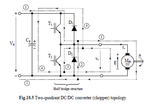
Hi i am working on dc motor drive using half bridge. The circuit is attached with this. IGBT i am using is stgw30nc120hd and and switching frequency is 20khz i am giving complementary signals to high side and low side igbt with 5us dead time.
the problem is the high side igbt getting heated and sometimes component fails.
I am also attaching the output current and voltage waveform.
from what i have read about the 2 qudrant chopper this waveform is not matching.
Can you guys give me some idea what is going on :)
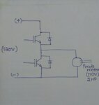
 

Hi,

no attachment.

And please post your complete schematic also.

Klaus
 
IMG_20160405_170039_1459855853680.jpgscope_2.png
 

Hi,

I seriously meant complete.
Without gate drive circuit it is impossible to analyse your problem.

Klaus
 

you must make sure your anti-parallel diodes are of the ultra fast or schottky type....very low reverse recovery time. If the igbt contains a diode then it must be low trr or you should choose another igbt

- - - Updated - - -

i would increase the dead time, and check those igbts can switch quick enough for 20khz operation....the current waveform looks very flat and id say you can switch at lower than 20khz and get away with it....you could try using fets instead. What is power?

- - - Updated - - -

but yes we do need to see gate drive cct to see if you are turning hard enough on and off.
 

The high side IGBT will surely get "heated" with respective motor current. What kind of heat sink do you provide? How much W/K?

The waveforms don't look unusual to me, except for 10 kHz rather than said 20 kHz switching frequency. Also probe scaling should be known.

I agree that MOSFETs can achieve lower losses at 120V supply and 10 or 20 kHz.
 

2q.pngwave.png

- - - Updated - - -

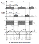
This is the theoritical graph. What i am getting is nowhere near this.
 

Hi,

This is the theoritical graph. What i am getting is nowhere near this.

Why not?

The upper two graphs show
*either the driving voltage
* or the voltage across the IGBTs

The lower is the current throgh the motor.

The voltageas are - in my eyes - what you see in post#3
But the current is not shown in post#3

Or is it the green line?
If so:
* Then in your circuit you have an offset because you only switch to positive side ... the externally driven voltage across the motor never becomes negative.
(only small negative voltage caused by the motor inductance and limited by the IGBT or the diodes)
* And if you switch the scope to AC mode and zoom in you will see the risng and falling current like in your post#7

Klaus
 

I presume the green trace shows the motor current. It is actually ramping, but current ripple is very low (high switching frequency + high motor inductance).

Instead of referring to a theoretical graph, how about estimating the expectable waveform for your drive?
 

In 3rd post the yellow colour graph is the voltage across lowside igbt.
and green colour is the output current (dso probe at dc coupling).
but why in my graph i am not getting the negative part of current waveform?
 

Hi,

but why in my graph i am not getting the negative part of current waveform?

* because you dont have negative voltage. So it can´t be forced to negative current.
* and you don´t break your motor. If you decrease your PWM frequency that low (maybe below 1 Hz), that during HIGH the motor is accelerated, then it will breaked when the PWM is LOW.
but your PWM frequency is much higher.. and you want uniform revolution....

(Fur sure in detail you may find negative voltage and current (spikes) )

Klaus
 

It's the motor emf that drives a negative current under circumstances. But a negative current would only flow if the motor inductance is much lower. It's not necessary for this configuration.

You don't want a ripple current that's more than 30% of the rated motor current, otherwise you get additional losses. If the motor is running with no load, negative instantaneous current is more likely to happen.
 
your waveforms look fine, though i didnt see any current limiting in your cct.
The actual drive method you are doing is kind of like a synchronous buck converter with 50% duty cycle drive.

The motor coil is effectively the buck inductor...and just as in a buck inductor in a synchronous buck that is loaded, the current does not go negative as long as the frequency is high enough, respectivley, the buck inductor of high enough henry value.
 
The Rce of your IGBT where Rce= (Vcc-Voh)/Ioh) or the effective ESR of the switch must be <5% of the motor winding resistance to minimize conduction losses in the high side driver.

The spec for stgw30nc120hd indicates ;
Vce_sat< 2.75V @30A @ 100'C or <2.75A @ 20A @ 25;C
p-n jcn. drops with rising T so Ice max drops when water cooled to 25'C

in any case at 100'C, Rce = 2.75V/30A = 92mΩ which generates I²R= 30² *0.092 = 83 Watts !!

You are probably not driving this much yet, as I suggested. Rce ought to be ~5% of load R which defines motor surge resistance (or DCR of Cu wire) when accelerating or braking. THis causes 5 to 8x times rated max current for motor is another way of determining DCR,

So with 15V for gate drive Vgs, this driver of approximately 0.1 Ohm supports a motor coil of about 2 Ohms for heavy surge currents. . What is your motor winding resistance?

Where are your calculations for power dissipation?

If it overheats with steady speed and low load, then you have timing issues with dead band, poor layout with crosswalk and ESL, poor CM noise interference or spurious resonance affecting SOA of the driver. (safe operating area) or poort thermal resistance between junction and ambient !!

What is your design verification for Rja and expected value ['C/W]? and expected loss W?

Try to measure driver output V vs I with differential probes on a 10 milliohm shunt. Balance probes for a flat line on scope when both on same switching V point using Ch A-B then move one probe to measure drop V for current from differential measurement.
Use twisted wire where possible or necessary and very short probe ground connections ( <1cm) with tip removed using probe barrel.

Then try to display as X vs Y for transient losses or better yet V*I on DSO for true power measurement.
 
Last edited:

    V

    Points: 2
    Helpful Answer Positive Rating
Status
Not open for further replies.

Part and Inventory Search

Welcome to EDABoard.com

Sponsor

Back
Top