Continue to Site

Welcome to EDAboard.com

Welcome to our site! EDAboard.com is an international Electronics Discussion Forum focused on EDA software, circuits, schematics, books, theory, papers, asic, pld, 8051, DSP, Network, RF, Analog Design, PCB, Service Manuals... and a whole lot more! To participate you need to register. Registration is free. Click here to register now.

Impedance Matching of RF Energy Harvesting System

Status
Not open for further replies.

Peiqii

Newbie level 6
Joined
Mar 10, 2016
Messages
13
Helped
0
Reputation
0
Reaction score
0
Trophy points
1
Activity points
91
Hi There,

I am going to do a RF energy-harvesting prototype system. However, I face some problems which are:

1. Which type of matching network (between Antenna and rectifier) is suggested to use?

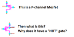
2. How to calculate the input impedance of the rectifier? The rectifier design is using the MOSFET transistor as the diagram below. I have no idea on calculating it.
FGCC.PNG
Kindly advise. Thanks!

Regards
Peiqii
 

It is too bad that your schematic is a negative image, is fuzzy, is covered in Chicken pox dots and has text so small that we cannot read it.
Why do some of your Mosfet symbols look weird with a "NOT" on its gate that I have never seen before?
 

Attachments

  • Mosfet symbols.png
    Mosfet symbols.png
    7.3 KB · Views: 96

Substrate diode arrow towards the channel is NMOSFET. Gate terminal with circle is a commonly used schematic notation for PMOSFET in ASIC schematics. You can of course argue about it's reasonability, I would take it as granted.

I completely agree about the poor readability of Cadence schematics, if the picture is blurred due to insufficient resolution on top of it, you should probably ignore the post.
 

Hi Dear,

So sorry for the negative image provided. Attached is the clear picture.
Screenshot1.png
I cant do anything with the chicken pox that you mentioned since i couldnt change it background.
BTW it is a common p-channel mosfet and you may search it in google.
left hand side is the nmos while right hand side is the pmos. It is the fully gate cross couple (FGCC) rectifier in 3 stages.
 

Hi

Hope this will help. The upper and lower terminal is connected to Vin+ and Vin- respectively. While the Vo1 is the output terminal.

Capture11.PNG
 

I believe that the rectifier circuit is wrong. Please check against literature. Synchronous rectification works with PMOS towards the positive output and NMOS for the negative branch.

Impedance matching at higher frequencies must take the transistor capacitance into consideration and varies over input and output voltage. Harmonic balance analysis is a straightforward method. Otherwise transient analysis with parametric sweeps.

Are you trying to match for a single frequency or a wider frequency range? In the former case, a standard LC filter (e.g. pi network) should work.
 

Hi FvM,

The literature showed this:
FGCC J.PNG

Btw I am a newbie in this field, do you have any tutorial or guideline or papers on how to calculate the input impedance of rectifier (with mosfet)? I hv no idea on how to start this part.

I didnt try to match this rectifier with antenna in simulation yet, but it will be use at 2.4GHz.

Thanks for the info.
 

but this is what i found in IEEE journal and there were many journal mentioned this topology.

May i know the purpose of swap the N1 and P2?

Please advise.
 

Sorry, I read your circuit wrong, confused by the + and - indication in your post. But you have AC input from top and bottom.

Everything O.K.

Back to the impedance problem, you need to define an output load resistor, than perform a transient analysis with 2.45 GHz sine source and vary the voltage in a parametric sweep. Then determine input current magnitude and phase and calculate input impedance. Or use harmonic balance if supported by your simulation tool.
 
  • Like
Reactions: Peiqii

    Peiqii

    Points: 2
    Helpful Answer Positive Rating
Is okay...

So may i know how to calculate the input impedance of this rectifier circuit?

Please advise.

- - - Updated - - -

okay...which mean that have to simulate it and then get the Vin and Iin, so based on that apply the Ohm's law to get the input impedance?
 

Basically ohms law, but expect a complex input impedance. Using a sine source is a simplification because voltage and current will have harmonics in the real application.
 

Thank you for posting clearer new schematics.

I am also confused by the odd looking Mosfet symbols in the book and in Cadence. The Mosfets are shown to have a separate substrate pin so maybe they are IC Mosfets and are not manufactured Mosfets that we buy. They show the arrow on the source pin but datasheets and Google show arrows on the substrate line that is always connected to the source pin. Now the N-channel Mosfets are upside down and are labelled "P1".

Maybe the Mosfets are actually right-side-up and are P-channel but have the arrow backwards?
 

Attachments

  • Cadence Mosfet.png
    Cadence Mosfet.png
    21.8 KB · Views: 97

Still some contradiction to your comments

1. The left most picture "your upside down N-channel MOSFET" shows a PMOSFET, as indicated by the letter P in designator and the source arrow towards the channel (= positive current flows into the source).
2. "This odd looking thing". MOSFETs with separate substrate terminal don't have a dedicated source. The source function is determined by the voltage polarity, similar to a junction FET.
 

Status
Not open for further replies.

Part and Inventory Search

Welcome to EDABoard.com

Sponsor

Back
Top