T
treez
Guest
Hello,
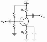
Do you know of a BJT with a really tightly toleranced hfe?
We only need it for Vce = 20V max and Ic = 10mA max.
[it will be used like in Q2 on page 25, fig31 of AN-47 (below)]
AN-47
https://ac-dc.power.com/sites/default/files/product-docs/an47.pdf
Do you know of a BJT with a really tightly toleranced hfe?
We only need it for Vce = 20V max and Ic = 10mA max.
[it will be used like in Q2 on page 25, fig31 of AN-47 (below)]
AN-47
https://ac-dc.power.com/sites/default/files/product-docs/an47.pdf