Continue to Site

Welcome to EDAboard.com

Welcome to our site! EDAboard.com is an international Electronics Discussion Forum focused on EDA software, circuits, schematics, books, theory, papers, asic, pld, 8051, DSP, Network, RF, Analog Design, PCB, Service Manuals... and a whole lot more! To participate you need to register. Registration is free. Click here to register now.

Power Amplifier Design for Bluetooth Applications

Status
Not open for further replies.

flames4791

Junior Member level 3
Joined
Nov 21, 2015
Messages
25
Helped
0
Reputation
0
Reaction score
0
Trophy points
1
Activity points
195
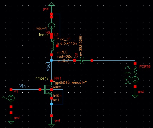
Hi, I need to design a power amplifier for a RF transmitter and I am not sure how to start. I have the VCO built and I was told that the output of the VCO needs to go to the power amplifier. I was also told that a class AB amplifier is a good topology but I am not sure how to build this. I googled it and theres so many different class AB and i dont know which is correct. Also, would the VCO connect to the gate of the PA transistor? I need to have 15 db gain, -10db output matching, decent linearity and output power, and 2.35 to 2.55GHz operating frequency. Any help would be greatly appreciated, thanks.
 

You need to design a mixer which upconverts the baseband signal using the VCO output. The output of the mixer should go to the PA. Start with class AB topology and based on the output resistor you are driving, do the calculations to find all the parameters like output swing and LC tank values etc.
 

You need to design a mixer which upconverts the baseband signal using the VCO output. The output of the mixer should go to the PA. Start with class AB topology and based on the output resistor you are driving, do the calculations to find all the parameters like output swing and LC tank values etc.

I was told by my professor to connect the vco to the PA because that is how the bluetooth architecture is supposed to be.
 

OK then are you modulating the vco output? And what kind of modulation are you designing the circuit for?
 

OK then are you modulating the vco output? And what kind of modulation are you designing the circuit for?

All I have done right now is a vco design. I dont know where to go from there
 

Either you need a mixer for upconversion or you need to generate a modulated VCO output(in case you are directly connecting the VCO output to PA) in order to be able to transmit using PA.
 

Either you need a mixer for upconversion or you need to generate a modulated VCO output(in case you are directly connecting the VCO output to PA) in order to be able to transmit using PA.

oh i guess i neeed to look more into it
 

So I am just trying to build the power amplifier on its own for now using the class A topology. I am not sure how to run output power and output p1db simulations on Cadence ADE. I was able to run output p1db but I am not sure if my setup is correct. I had just one port, which was placed at the output and then I ran a PSS simulation and plotted the output 1db compression of the port. Can anyone confirm that that is how to run the simulation? Also, what are ways to get better output p1db, as i need to have above 3dbm.


Status
Not open for further replies.

Part and Inventory Search

Welcome to EDABoard.com

Sponsor

Back
Top