prateek3790
Full Member level 2
i am trying to match my antenna by using a lumped matching network.
i fed the antenna using a lambda/12(using fr-4 @2.4ghz)line the thickness of the substrate i used is 3.6 mil and z0=50ohm.
i calculated the dimension using this.(see the link below)
https://www.emtalk.com/mscalc.php?e...ts_list=Wmm&La=5.70811941473&L_units_list=Lmm.
then i used a lumped port and found the impedance seen by the port using active z (re and im).
my zin=0.05+j33.36.
so to match this to 50 ohm i used a l lumped network where the component value i determined using (see the link below)
https://home.sandiego.edu/~ekim/e194rfs01/jwmatcher/matcher2.html
(used the first ckt)
c=1.894pf and l=0.109nH.
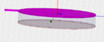
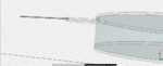
i drew the rlc boundary for capacitor and connected it to previous geometry(tr line of lambda/12 included) the other end of this c boundary is connected to another tr line of same specification.
both tr line have same ground plane.inductor is connected to one end of capacitor boundary and ground to the another.
after doing this when again i used the lumped port to find the zin it gives the same value as previous one.
means it is not matched. but why???
i just extended the the metal and ground of the second line by small value to provide separation between the inductor boundary and second line. but removing this gap also do not helped.getting the same zin.


 .
.
see the images to check the connection of tr_line with the matching networks.
i am using driven model.
new to hfss so don't know whether this much info is enough or not
i fed the antenna using a lambda/12(using fr-4 @2.4ghz)line the thickness of the substrate i used is 3.6 mil and z0=50ohm.
i calculated the dimension using this.(see the link below)
https://www.emtalk.com/mscalc.php?e...ts_list=Wmm&La=5.70811941473&L_units_list=Lmm.
then i used a lumped port and found the impedance seen by the port using active z (re and im).
my zin=0.05+j33.36.
so to match this to 50 ohm i used a l lumped network where the component value i determined using (see the link below)
https://home.sandiego.edu/~ekim/e194rfs01/jwmatcher/matcher2.html
(used the first ckt)
c=1.894pf and l=0.109nH.
i drew the rlc boundary for capacitor and connected it to previous geometry(tr line of lambda/12 included) the other end of this c boundary is connected to another tr line of same specification.
both tr line have same ground plane.inductor is connected to one end of capacitor boundary and ground to the another.
after doing this when again i used the lumped port to find the zin it gives the same value as previous one.
means it is not matched. but why???
i just extended the the metal and ground of the second line by small value to provide separation between the inductor boundary and second line. but removing this gap also do not helped.getting the same zin.
.see the images to check the connection of tr_line with the matching networks.
i am using driven model.
new to hfss so don't know whether this much info is enough or not

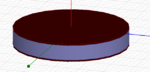
_w=2mm_l=5mm_h=0.3mm.PNG")
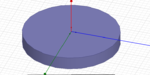
_r=11.5mm,h=-3mm.PNG")