Continue to Site

Welcome to EDAboard.com

Welcome to our site! EDAboard.com is an international Electronics Discussion Forum focused on EDA software, circuits, schematics, books, theory, papers, asic, pld, 8051, DSP, Network, RF, Analog Design, PCB, Service Manuals... and a whole lot more! To participate you need to register. Registration is free. Click here to register now.

Operation of Bandpass active filter

Status
Not open for further replies.

wherati

Newbie level 5
Joined
Jan 19, 2016
Messages
8
Helped
1
Reputation
2
Reaction score
1
Trophy points
3
Activity points
94
BandPass.jpg
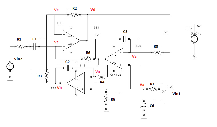
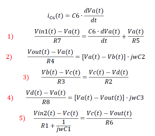
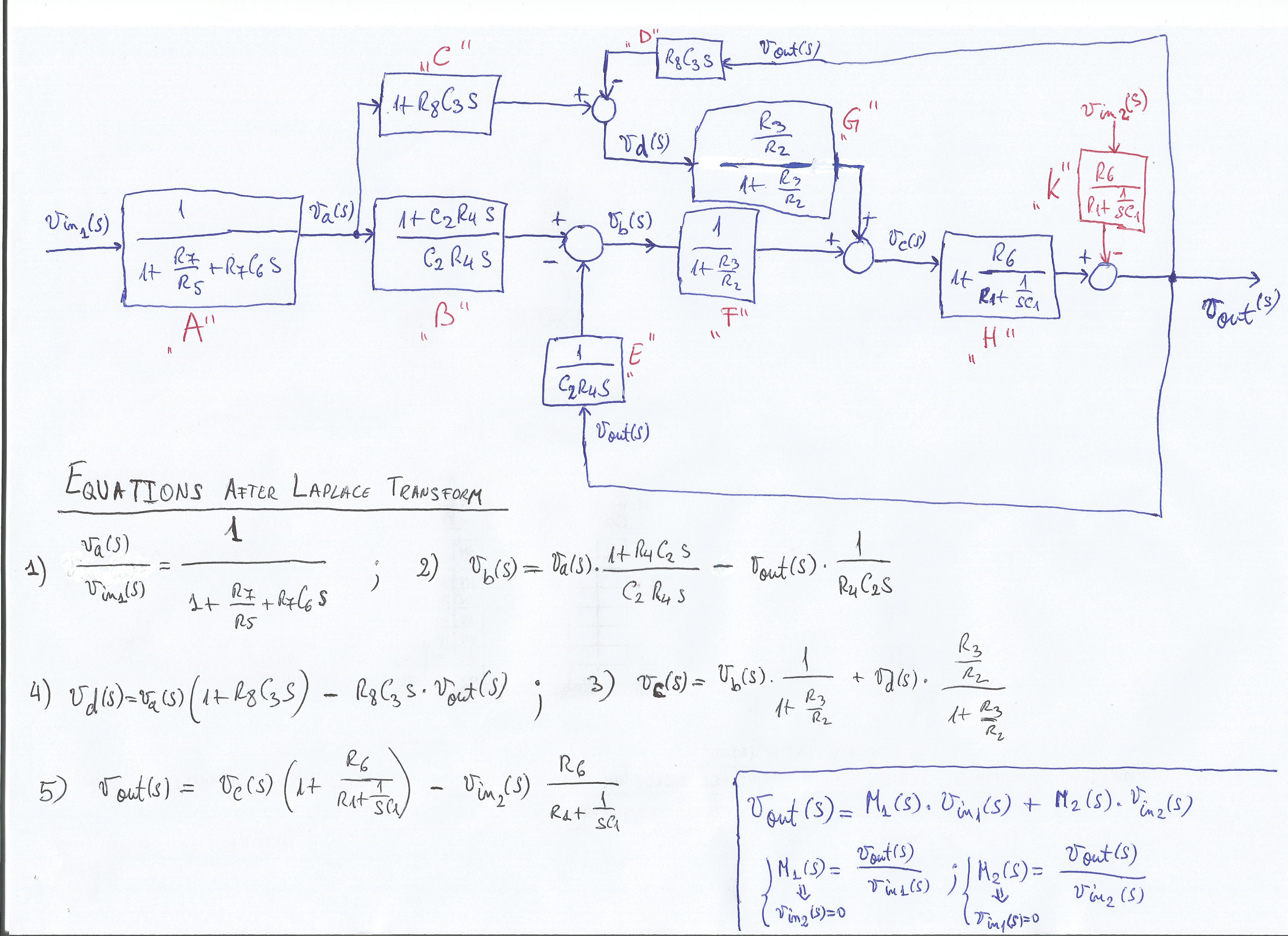
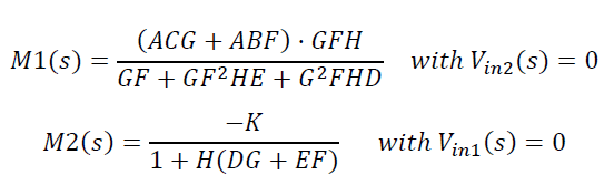
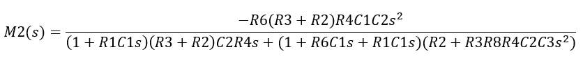
I am having a hard time understanding the operation of this bandpass filter - i.e. the qualitative operation of the feedback which would allow me to determine what sets F0, Q and gain. I think the two lower opamps operate as integrators centered around Vcc/2, but the rest of the loop has me kind of baffled.
 

Two inverting integrators - together with an amplifier - form a closed-loop which is known as KHN topology.
Both integrator outputs are fed back to the non-inv. and invertimg opamp input terminals, respectively.
You should consult a textbook or some other sources using the keyword "KHN Filter".
 
Two integrators with feedback make a second order differential equation, I think the correspondence is quite intuitive, also how to tune f0 and Q by varying resistors.

- - - Updated - - -

See I was a bit late. One more thing, state variable filter is also a descriptive name for the topology.
 

One more thing, state variable filter is also a descriptive name for the topology.

I think, the topology under question is ONE of some other state-variable structures (e.g. Tow-Thomas, Fleischer-Tow, Akerberg-Mossberg,..)
 

I have tried to analyze the circuit theoretically and get the transfer function, place the feedback etc.. but I am stucked. How did you analyze it?

I tried assuming the OP amps are ideals.


When I place the equations, it is not possible to find the transfer function, I mean, there are 3 unknown variables instead of 2...


NOTE: I have just realised that I have called a capacitor C6 instead of C4 :bang:
 

What you are noting as Vin1(t) is just Vcc, used to bring up the DC to Vcc/2 through the 100k dividers. I should probably have been more explicit than just marking it with 5V in my original schematic. I was also negligent in not pointing out that V- is connected to ground, as we are operating with a single supply.

I addition, I think we can also assume R8=R4 and C3=C2.

Finally, I believe C6 doesn't play any role in the response - it's just a bypass cap for the Vcc/2 bias point.
 
Last edited:
  • Like
Reactions: CataM

    CataM

    Points: 2
    Helpful Answer Positive Rating
For a principle analysis, you can also omit the input coupling capacitor which adds a highpass function that doesn't belong to the basic filter transfer function. Doing so, you get the expected ideal highpass transfer function.

sapwin.png
 
I should probably have been more explicit than just marking it with 5V in my original schematic. I was also negligent in not pointing out that V- is connected to ground, as we are operating with a single supply.

-Yes I saw that, but I tried to the analysis like there were 2 inputs.
-What do you mean with "V-" ? "V-" of the OP amps ? or of the 5 V supply ?


Finally I have made the analysis and wasn't that hard. The only staff was that I have forgotten that is a feedbacked circuit and could not do it, but the feedback simplifies the implementation of the blocks.

This is the result ( I called the blocks A,B,C.. to refer easier to them).


On the right corner of the paper, I found out the Vout(s) by using SUPERPOSITION THEOREM, and M2(s) is the transfer function that FvM showed (with Vin1=0).

M1(s) and M2(s) expresiones are like this if I am not wrong:


Seeing the blocks I have some questions:

1) OP amps usually are working in linear zone where Superposition Theorem can be applicable. But how do we know that this one is not working in the non-linear zone?

2) Blocks "C" and "D" have more zeroes than poles, which is not possible in LTI (linear time invariant) systems. How is that possible ? MATLAB do not accept to implement that kind of blocks to simulate it.
 
Last edited:

1) OP amps usually are working in linear zone where Superposition Theorem can be applicable. But how do we know that this one is not working in the non-linear zone?

2) Blocks "C" and "D" have more zeroes than poles, which is not possible in LTI (linear time invariant) systems. How is that possible ? MATLAB do not accept to implement that kind of blocks to simulate it.
1. The complete analysis is based on linear network theory., it's valid as long as the OPs don't run into slew rate limitations or saturation. Please consider that you assumed ideal OPs, adding finite gain and bandwidth to the simulation would be the first step towards an exact analysis.

2. I'm unable to identify the zeros in the post #5 schematic, I presume an analysis error.

Calculating a transfer function for the "Vin1" reference input is surely possible, but what's the purpose?
 
  • Like
Reactions: CataM

    CataM

    Points: 2
    Helpful Answer Positive Rating
2. I'm unable to identify the zeros in the post #5 schematic, I presume an analysis error.

Calculating a transfer function for the "Vin1" reference input is surely possible, but what's the purpose?

The zeros comes from equation 4. Even though there are capacitors, to implement the transfer functions, I must use variables "known" or founded by combination.
In equation 4, I have Va(s) and Vout(s), so I can get Vd(s) and go on drawing more blocks. Having Vd(s) I can find out Vc(s) in equation 3 and so on...

The transfer function for Vin1 was just to practice... Nevertheless I did not know each one purpose (Vin1 and Vin2) before you explained them.
 

First off, I really appreciate the obviously great amount of effort you've all put into this question. Thank you!

V- refers to the negative supply voltage, which should be connected to ground, which I hoped to clarify by the 'Single Supply' comment. I'm not sure, though, of the benefits of considering Vin1 as another input, as that certainly will complicate matters. In my derivation, where I replace each integrator with a 1/sRC response, I am able to get a biquad equation with a single zero at DC corresponding to the R1C1 pair, but both the damping factor and natural frequency involve a combination of almost all the resistors and capacitors. This makes it impossible to decouple Q factor, resonant frequency and gain - though I think there's a good likelihood I may have an error in my algebra. Is it possible that this configuration does not allow for separately setting Gain,Q and Wn - ie. it does not have enough degrees of freedom? With the values indicated in the original schematic, I simulate a resonance at around 3.25kHz and a Q of 50 for a gain of about 41.7dB.

I like FvM's suggestion of ignoring the zero caused by C1, as that will be at very low frequency anyway and is not really a part of the filter itself. Will try to proceed along that line.
 

In equation 4, I have Va(s) and Vout(s), so I can get Vd(s)
The signal flow is taking the opposite direction, there's no actual zero in the transfer function.

This makes it impossible to decouple Q factor, resonant frequency and gain - though I think there's a good likelihood I may have an error in my algebra. Is it possible that this configuration does not allow for separately setting Gain,Q and Wn
The parameters can be set independently, but not by changing a single resistor. There are slightly different double-integrator filter topologies where you can change Q and G with a single resistor, each. To tune ω independently, you need a dual variable resistor in any case.
 

In my derivation, where I replace each integrator with a 1/sRC response, I am able to get a biquad equation with a single zero at DC corresponding to the R1C1 pair, but both the damping factor and natural frequency involve a combination of almost all the resistors and capacitors.

That is working with 3 capacitors(C1, C2 and C3) ?
The order of the transfer function if working with 3 capacitors must be 3, because the order of a transfer function is the number of storing energy elements of a circuit.

Working with Vin1=0, my transfer function is like this (3rd order):


If you are going to work as FvM said, then the order of the transfer function is 2 just as he showed.
 
Last edited:

As mentioned before, the circuit is well known; it is the popular KHN biquad.
It is a second-order filter and the shown output provides a bandpass function.
The input capacitor (C1) is not part of the filter function and its value is chosen very large in order not to influence the desired characteristics.
What is the problem now?
 
Last edited:

@FvM, thanks. At this point, I am able to derive the 2nd order H(s) for the filter much like you did.

By writing H(s) as: (alpha * s)/(s^2 + beta * s + gamma), where alpha, beta and gamma are functions of the R's and C's, the Bode plot of H(s) in Octave agrees with Spice sim of the circuit. However, as you indicated also, beta (wn/Q) and gamma (wn^2) are coupled in terms of the R's and C's but I think it is possible to decouple them - though not very obvious at a glance.
 

The mutual dependency of component values can be reduced by adding a fourth OP so that all can be operated in inverting configuration.
 
That sounds very insightful. Can you please elaborate on how adding a fourth OpAmp (I assume without adding another pole) helps the degrees of freedom?
 

Degree of freedom isn't the problem, you can calculate component values for arbitrary combinations of ω0, Q and G. But the non-inverting configuration of the summing amplifier makes it necessary to modify multiple resistor values to change a parameter. That's no problem for a fixed filter, but if you want e.g. to adjust filter Q independent of other paraeters, a four OP circuit has advantages.
 

I set R4 = R8 = R, and C2 = C3 = C (both integrators have same values), and simplify and get:

Gain: -R6/R1
Wn: sqrt(R2/R3) / (R*C)
Q = sqrt(R3/R2) * (1 + R6/R1) * (1 / (1 + R3 / R2) )

The values in the circuit are:

R1 = 100
R6 = 10M
R2 = 100k
R3 = 10k
R = 470k
C = 0.33p

With the above, I get:

Gain = 10^7 / 100 = 100dB (matches spice sim reasonably enough)
Wn = sqrt(10) / (470e3 * 0.33e-9) = 20.38e3 Rad/s = 3.245kHz (matches spice sim)
Q = sqrt(0.1) * (1 + 10^5) * 1 / (1 + 0.1) = 28.7k (???)

That Q values doesn't make sense ... I think it should be somewhere between 50 and 100?? Of course, I am computing with ideal opamp parameters here, but that seems way way off! I'm trying to get this filter centered around 1K with a Q of about 10 and gain of 40dB.

I don't mind tweaking multiple resistors to tune this filter, and prefer that to using another opamp.
 

As far as I see correctly calculated, except for the capacitance value which should be 330 pF.

G=10e5 and the respective Q value are purely fictional. Instead you'll put in the intended gain which fixes R6/R1 and need to adjust R3/R2 to achieve the specified Q. Unfortunately, you get a dynamic range problem with this circuit if you make G considerably larger than Q. One more reason to use a different topology. Or to implement part of the gain outside the filter.

I found an apparently better considered three OP circuit https://en.wikipedia.org/wiki/State_variable_filter
 

Status
Not open for further replies.

Similar threads

Part and Inventory Search

Welcome to EDABoard.com

Sponsor

Back
Top