Continue to Site

Welcome to EDAboard.com

Welcome to our site! EDAboard.com is an international Electronics Discussion Forum focused on EDA software, circuits, schematics, books, theory, papers, asic, pld, 8051, DSP, Network, RF, Analog Design, PCB, Service Manuals... and a whole lot more! To participate you need to register. Registration is free. Click here to register now.

Rf power amplifier design

Status
Not open for further replies.

aks.rfms

Junior Member level 2
Joined
Apr 28, 2014
Messages
24
Helped
0
Reputation
0
Reaction score
0
Trophy points
1
Activity points
196
I have design an power amplifier , in simulation its showing proper result but after fabrication , i mount it on heat sink.

The rated specification are

--LDMOS device free-scale.
-- drain voltage -- 28 Volt
-- Gate voltage -- 3.8 volt
-- rated Input -- 21 dBm
-- rated output -- 45 dBm
-- gain -- 23 dB
-- optimum current -- 330mA.


but after mounting...

i give 28 Volt drain side , but as i raise the voltage to gate side about 2.8 Volt it went into oscillation,

i provide proper vias for grounding even after it show the 33 dBm out put ,without any rf input (in biasing condition only), and shows current of 300 mA.

it does not show any effete even i give rf to optimum input level.


kindly guide me to get out of oscillation and get proper out put..

thanking you
 

you should connect tantalum capacitor for output side.
 

There is some thing wrong with layout or decoupling, because some of the output power is getting into the input circuitry. So make sure that the Vcc is properly decoupled from SHF down to AF, put a screen between the input and output which is earthed. It would help if we knew what the design frequencies was and the oscillating frequency.
Frank
 

i connected the tantalum capacitor both at input and output supply side only.
but i facing the same problem.
 

Forget the tantalum capcitor idea. You have unwanted coupling from the output side to an earlier stage of the amplifier or to the device driving it. As Frank points out, you may have to physically shield the in and out ends from each other or you might have signals travelling along wiring shared between stages. We need to know:

1. What frequency is it supposed to amplify at?
2. what frequency is it oscillating at?
3. If possible a schematic and photograph of the layout you have used.

Brian.
 
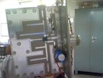
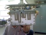
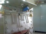
Post a picture of your practical amplifier implementation here..
 

freq. to amplify - 1300MHz
oscillation freq.- 1300 MHz +/- 100 MHz bandwidth

Pic is showing error while uploading.

will trying and upload earliest.
Picture 006.jpgPicture 005.jpgPicture 003.jpg
 

The layout and board construction look excellent. The only thing I can't confirm from the pictures is whether there are PTH along the center track (assume this is the source pins) so they are linked to the backplane. I also can't see if the input and output sockets are grounded to the visible side of the board.

If it still oscillates, the only options I can think of are to add a screen across the top of the LDMOS to limit magnetic coupling between input and output or to add a neutralizing network althogh that would tend to reduce the gain somewhat.

Brian.
 

The layout does not seem very proper.
There are 2 GND field and there are connected with a narrow copper lines while they are underpassing the transistor.These lines will act as an inductor at the source/emitter of the transistor and the amplifier will probably oscillate.
The power transistors are not connected in that way. Look at especially Freescale ANs to get correct information about a proper layout.
 

I will upload the more clear pic for the same....kindly suggest me more ..

- - - Updated - - -

Rf power amplifier design

In my another design...after fabrication , I got parameters as follows:

S11 = -0.6779dB
S11(Ω)= 43.5-j233.7 Ω

S21= +19.36 dB (gain)
S12= -28 dB

S22 = -20.31 dB
S22 (Ω)= +49.2+j9.8 Ω


The Problem is that , the gain is received at 0 dBm but as i increase the input power level to its rated input at 20 dB from source , the expected output from this is about 40 dBm.

the device for the mention model is 25 watts (45 dBm)


but it get saturated at 36 dBm.

As per my perception, i feel that as the input return loss is very poor in imaginary part,
most of the power is reflected back to the source from the input of the amplifier.


Kindly let me know and suggest , whether i am correct? then how to design the compensation network for the imaginary part of the impedance.


if not then what may be the cause.
and then how to resolve that .


thanking you
 

Status
Not open for further replies.

Part and Inventory Search

Welcome to EDABoard.com

Sponsor

Back
Top