Continue to Site

Welcome to EDAboard.com

Welcome to our site! EDAboard.com is an international Electronics Discussion Forum focused on EDA software, circuits, schematics, books, theory, papers, asic, pld, 8051, DSP, Network, RF, Analog Design, PCB, Service Manuals... and a whole lot more! To participate you need to register. Registration is free. Click here to register now.

[SOLVED] designing structured vhdl code up _down counter

Status
Not open for further replies.

Eli_221B

Newbie level 4
Joined
Dec 20, 2015
Messages
6
Helped
0
Reputation
0
Reaction score
0
Trophy points
1
Activity points
50
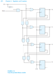
hello every one:wink: I have serious problems in writting vhdl structural 4 bit up/down binary counter code by 4 t flip flops.... this is my first code Im so confused and havent enough time. please help and guide me to learn and edit it . thank you so much
1.png


Code VHDL - [expand]
1
2
3
4
5
6
7
8
9
10
11
12
13
14
15
16
17
18
19
20
21
22
23
24
25
26
27
28
29
30
31
32
33
34
35
36
37
38
39
40
41
42
43
44
45
46
47
48
49
50
51
52
53
54
55
56
57
58
59
60
61
62
63
64
65
library ieee; 
use ieee.std_logic_1164.all;
 entity tff is
 port ( t :in std_logic;
 clock :in std_logic;
 reset :in std_logic;
 q :out std_logic
 );
 end entity;
 architecture behavior of tff is
 signal s :std_logic;
 begin
 process (clock) 
 begin
 if (clock'event and clock='1') then
 if (reset = '0') then 
 s <= '0';
 else s <= not s; 
 end if; 
 end if; 
 end process; 
 q <= s; 
 end architecture;


---------------------------------------------------------
library IEEE;
use IEEE.STD_LOGIC_1164.ALL;
 
entity up_down_structure is
port( up:in std_logic;
down:in std_logic;
clock:in std_logic;
a0,a1,a2,a3:inout std_logic);
end entity;
 
architecture structural of up_down_structure is
 
component tff is
port( t: in std_logic;
clock:in std_logic;
q:out std_logic;
qbar:inout std_logic);
end component;
 
signal t1,t2,t3,t4,t5,t6,t7,or_1,or_2,or_3,or_4,qbar1,qbar2,qbar3:std_logic;
begin
t1 <= ((not up) and down);
t2 <=  t1 and qbar1;
t3 <= up and a0;
t4 <= t2 and qbar2;
t5 <= t3 and a1;
t6 <= t4 and qbar3;
t7 <= t5 and a2;
or_1 <= up or t1;
or_2 <= t2 or t3;
or_3 <= t4 or t5;
or_4 <= t6 or t7;
 
t_ff1:tff port map(or_1 =>t,clock =>clock, q =>a0);
t_ff2:tff port map(or_2 =>t,clock => clock,q =>a1);
t_ff3:tff port map(or_3 =>t,clock => clock,q=>a2);
t_ff4:tff port map(or_4 =>t,clock => clock,q =>a3);
end architecture;

 
Last edited by a moderator:

What exactly is the peoblem? other than a tedious and not very useful problem (I assume set by some professor?)
 

Your tff component doesn't work, because input t isn't used in the logic. And it won't compile in your design because it has an unconnected reset input without default value.
 
that was a good explanation thanks. but what should I do? can someone gives a correct code or correct it?
 

Try
Code:
 entity tff is
 port ( t :in std_logic;
   clock :in std_logic;
   reset :in std_logic := '1';
   q :out std_logic
 );
 end entity;
 architecture behavior of tff is
   signal s :std_logic;
 begin
   process (clock) 
     begin
       if (clock'event and clock='1') then
         if (reset = '0') then 
           s <= '0';
         elsif t='1' then
           s <= not s; 
         end if; 
       end if; 
     end process; 
     q <= s; 
 end architecture;

I didn't check the counter logic itself.

A full "structural" design would also involve components for the AND and OR gates.
 
hello every one:wink: I have serious problems in writting vhdl structural 4 bit up/down binary counter code by 4 t flip flops.... this is my first code Im so confused and havent enough time. please help and guide me to learn and edit it . thank you so much

I suggest you take your picture of the circuit and name all the signals that connect between the gates/TFFs, that aren't currently named, and name all the TFF/gates in the drawing.

Make VHDL files for each type of component AND/OR/INVERT/TFF.

Add an instances in a top level VHDL file for each gate/TFF in the structural drawing using the names for the gates/TFFs you added earlier. For each port of each gate/TFF, add the name you used in the drawing that connects to that port.

If you do this you'll have the exact circuit you show in the drawing...i.e. you'll be describing the hardware.

FYI you have an error in the following statements:

Code VHDL - [expand]
1
2
3
4
t_ff1:tff port map(or_1 =>t,clock =>clock, q =>a0);
t_ff2:tff port map(or_2 =>t,clock => clock,q =>a1);
t_ff3:tff port map(or_3 =>t,clock => clock,q=>a2);
t_ff4:tff port map(or_4 =>t,clock => clock,q =>a3);


All the ports for t are swapped. It should be t => or_#
 
thank you for your time FVM and ads_ee :)
I’v corrected t=>or_# :thumbsup:
this is the pic with signals I’v specified
1.png
and these are new errors, why reset errors?
what about and/or components should I use? or does it need a clock divider?
13.jpg

- - - Updated - - -

14.jpg
only line 79 has problem with reset?
 

There's no reset signal in your diagram, so it should neither appear in your HDL, isn't it?

If you have it though, e.g. because you used a given FF template, you should connect it respectively to satisfy the language syntax requirements.
 
You should probably remove the reset from your TFF file and add a initial value for the s signal
signal s :std_logic := '0';
to avoid X's in simulation.

You also neglected to add a QB output to the TFF (which is in your drawing) and did not label that QB signal on the drawing.
 
i dont know how connect qbar? to what?:sad:
removing reset doesnt work
 

The suggestion was to add qbar to the TFF component, e.g.
Code:
qbar <= not s;

I don't understand what's the present problem with reset.
 
yess got it :-D
& I’v added reset input which was undefined in t component and entity
tnx every body :thumbsup:
wish the best,happy christmas
 

Status
Not open for further replies.

Part and Inventory Search

Welcome to EDABoard.com

Sponsor

Back
Top