Continue to Site

Welcome to EDAboard.com

Welcome to our site! EDAboard.com is an international Electronics Discussion Forum focused on EDA software, circuits, schematics, books, theory, papers, asic, pld, 8051, DSP, Network, RF, Analog Design, PCB, Service Manuals... and a whole lot more! To participate you need to register. Registration is free. Click here to register now.

comparison a logic gate performance based on mosfet and ofet

Status
Not open for further replies.

electronicman26

Full Member level 2
Joined
Dec 15, 2011
Messages
120
Helped
2
Reputation
4
Reaction score
2
Trophy points
1,298
Activity points
2,054
Hi
I want to compare a logic gate (for example nand,or,and,not,...) performance based on mosfet with the same based on ofet
now I have several question:
1-should the circuit topology be same in mosfet and ofet based?
2-is it correct that compare 0.18um mosfet with ofet that has 25um length?
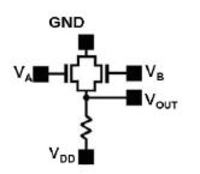
 

It seems kind of kooky to pick a 0.18um MOSFET as your
point of comparison. What makes these two, anything like
equivalent? Supply voltage? Certainly not form factor.

Does your "ofet" have a N and P species? If not, your
logic gate topology will differ and the comparo would be
even less relevant. What devices do you have at hand?

I think it would be good to at least try to match
technologies by working voltage.
 
I use OPDK (organic process designkit) based on Ion-Gel Gated, the operating voltage(supply) is low (1 or 2 volt), and just has p type and is not complementary
http://opdk.umn.edu/index.html
0.18um supply voltage is 1.8 or 2 volt
now do you think that the comparison between them is correct and acceptable??
How can I find the minimum length that is acceptable for this type of ofet??
 

Min geometry would come from whoever's printing it
(wafer fab? silk screen?) and what they know about
manufacturability, reliability.

The 1.8V MOSFET (PMOS) may be your best bet as
a comparison, but perhaps it's more about gate oxide
(dielectric) thickness - you can operate thicker oxide,
5V or higher, FETs at 1.8V and since Cox is a big deal
in channel conductance and gm, matching tox might
be more fair. But the paper I looked through at that
link provided only L, W and no gate thickness I could
see. Your minimum L, for comparo purposes, should be
5um (not 0.18um) or higher - whatever the discussed
gates' ring oscillator performance was based upon,
geometry-wise.

The logic style shown is PMOS depletion-load. Very
similar to the first MOS products, before they got a
handle on the various reliability detractors (PMOS
"walks out" leakage and breakdown while NMOS
"walks in" from hot carrier and mobile ion charge).
Look for info on old-timey PMOS logic and maybe
you will find some interesting side references. But
the http://opdk.umn.edu/files/AFM10_OFET.pdf
paper looks to have enough circuit detail for you
to replicate their work using silicon PMOS devices.
 
now I just want to do simulation to compare the simulation results, and it is impossible for me to build. but I want my simulation be close to reality.
conclusion of above discuss:
for OFET I use opdk designkit, the minimum L that can use is 5um, and just have p-channel OFET then the topology must be selected based on p-channel transistor.
for Mosfet I use TSMC 0.18um designkit, the minimum L that can use is 0.18um, that have both p and n channel Mosfet but for better comparison the topology select based on p-channel.
Is it better to have exactly the same circuit topology for this two technology??
for example:

in this way, if I want to have a table for comparison the OFET nand gate and the Mosfet based nand gate, which parameters is good for this compare? and which parameters should be calculate?
 

Well, what do you want from this "comparison"? You could,
after all, "compare" a Viking longboat to a jet-ski. They
both float,after all. But comparisons like this are not
especially fruitful or relevant. I'd back up a step or two,
figure what dimensions of performance, reliability, cost
and so on matter, and then think about how (or whether)
you would indeed apply a 0.18um silicon foundry technology
to any problem that overlaps OFET viability, then why and
how. Maybe a more mature and lower cost technology is
more in line with interests than a 0.18 product development
(which ought to soak you for at least $100K on a multiproject
lot, which can't support production and will require more like
$500K for your own tooling and first article wafer lot). If
the interest in OFET is flexible / printable circuitry, the
foundry wafer is the beginning and not the end - wafer
thinning and attachment / encapsulation of thinned die
will be the next steps, each has their own development
phase before they can yield useful feedstock for whatever
the larger picture is, etc.).

Anyhow, look to the values-set for basis of comparison,
and to what.
 
my target is to show that the ion-jel OTFT (with the use of OPDK transistors for simulation) is good for logic circuit design or no,
what is your suggest for doing this?
how can I find that the OFETs are good for logic circuit design or no?
 

"Good"? That depends. Mostly on what your alternatives
are. Back in the day, bipolar logic was "good" - slow,
power hungry, limited density, but still better than the
even-slower and not-much-less-hungry depletion-load
PMOS (NMOS having yet to become reliable). Only when
CMOS reached the 3um range, did it become performance
competitive and win on power.

Back to the point, OFETs may well be "good" for logic
when you have no desirable alternative and sufficiently
low expectations for speed, density and so on. Perhaps
the end game is a low cost printed active electronics
thing, that you just don't want to flip-chip a silicon die
onto. Perhaps that also can stand a <1MHz clock and
a few hundred transistor count. In this case, maybe
OFETs are "perfect".

But as a straight up alternative to a 1Mgate, 500MHz
main clock CMOS logic device? No way. And comparison
on this basis will surely say so.

I think I would try to express the applications where
OFETs do make sense, and derive their limitations from
your circuit analysis and higher order analyses (density,
cost, etc.). Your matchup to 0.18u CMOS may be an
anecdote that supports some part of the story. But I
think it is far off from the main thrust of the story,
that being "what use is an OFET, thusly made?".
 

Status
Not open for further replies.

Part and Inventory Search

Welcome to EDABoard.com

Sponsor

Back
Top